ZHCSIY5A October 2018 – May 2019 LMZM33604
PRODUCTION DATA.
- 1 特性
- 2 应用
- 3 说明
- 4 修订历史记录
- 5 Pin Configuration and Functions
- 6 Specifications
-
7 Detailed Description
- 7.1 Overview
- 7.2 Functional Block Diagram
- 7.3
Feature Description
- 7.3.1 Adjusting the Output Voltage
- 7.3.2 Input Capacitor Selection
- 7.3.3 Output Capacitor Selection
- 7.3.4 Transient Response
- 7.3.5 Feed-Forward Capacitor
- 7.3.6 Switching Frequency (RT)
- 7.3.7 Synchronization (SYNC/MODE)
- 7.3.8 Output Enable (EN)
- 7.3.9 Programmable System UVLO (EN)
- 7.3.10 Internal LDO and BIAS_SEL
- 7.3.11 Power Good (PGOOD) and Power Good Pullup (PGOOD_PU)
- 7.3.12 Mode Select (Auto or FPWM)
- 7.3.13 Soft Start and Voltage Tracking
- 7.3.14 Voltage Dropout
- 7.3.15 Overcurrent Protection (OCP)
- 7.3.16 Thermal Shutdown
- 7.4 Device Functional Modes
- 8 Application and Implementation
- 9 Power Supply Recommendations
- 10Layout
- 11器件和文档支持
- 12机械、封装和可订购信息
7.3.8 Output Enable (EN)
The voltage on the EN pin provides electrical ON/OFF control of the device. Once the EN pin voltage exceeds the threshold voltage, the device starts operation. If the EN pin voltage is pulled below the threshold voltage, the regulator stops switching and enters low quiescent current state.
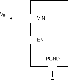
The EN pin cannot be open circuit or floating. The simplest way to enable the operation of the LMZM33604 is to connect the EN pin to VIN directly as shown in Figure 33. This allows self-start-up of the LMZM33604 when VIN reaches the turn-on threshold.
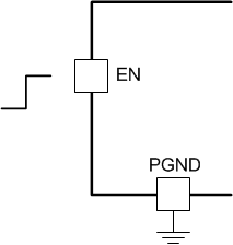
If an application requires controlling the EN pin, an external logic signal can be used to drive EN pin as shown in Figure 34. Applications using an open drain/collector device to interface with this pin require a pullup resistor to a voltage above the enable threshold.
 Figure 33. Enabling the Device
  Figure 34. Typical Enable Control