SNVS764Q January 2000 – December 2017 LP2950-N , LP2951-N
PRODUCTION DATA.
- 1 Features
- 2 Applications
- 3 Description
- 4 Revision History
- 5 Voltage Options
- 6 Pin Configuration and Functions
- 7 Specifications
-
8 Detailed Description
- 8.1 Overview
- 8.2 Functional Block Diagrams
- 8.3 Feature Description
- 8.4 Device Functional Modes
-
9 Application and Implementation
- 9.1 Application Information
- 9.2
Typical Applications
- 9.2.1 1-A Regulator with 1.2-V Dropout
- 9.2.2 300-mA Regulator with 0.75-V Dropout
- 9.2.3 Wide Input Voltage Range Current Limiter
- 9.2.4 Low Drift Current Source
- 9.2.5 5-V Current Limiter
- 9.2.6 Regulator with Early Warning and Auxiliary Output
- 9.2.7 Latch Off When Error Flag Occurs
- 9.2.8 2-A Low Dropout Regulator
- 9.2.9 5-V Regulator with 2.5-V Sleep Function
- 9.2.10 Open Circuit Detector for 4 → 20-mA Current Loop
- 9.2.11 Regulator with State-of-Charge Indicator
- 9.2.12 Low Battery Disconnect
- 9.2.13 System Overtemperature Protection Circuit
- 10Power Supply Recommendations
- 11Layout
- 12Device and Documentation Support
- 13Mechanical, Packaging, and Orderable Information
7 Specifications
7.1 Absolute Maximum Ratings
over operating free-air temperature range (unless otherwise noted)(1)(1)| MIN | MAX | UNIT | ||
|---|---|---|---|---|
| Input supply voltage - SHUTDOWN input voltage error comparator output voltage(2) | –0.3 | 30 | V | |
| FEEDBACK input voltage(2)(3) | –1.5 | 30 | V | |
| Power dissipation | Internally Limited | |||
| Junction temperature, TJ | 150 | °C | ||
| Soldering dwell time, temperature | Wave | 4 seconds, 260 | ||
| Infrared | 10 seconds, 240 | |||
| Vapor phase | 75 seconds, 219 | |||
| Storage temperature, Tstg | –65 | 150 | °C | |
(1) If Military/Aerospace specified devices are required, contact the Texas Instruments Sales Office/Distributors for availability and specifications.
(2) May exceed input supply voltage.
(3) When used in dual-supply systems where the output terminal sees loads returned to a negative supply, the output voltage should be diode-clamped to ground.
7.2 ESD Ratings
| VALUE | UNIT | ||||
|---|---|---|---|---|---|
| LP2950-N | |||||
| V(ESD) | Electrostatic discharge | Human-body model (HBM), per ANSI/ESDA/JEDEC JS-001(1) | ±2500 | V | |
| LP2951-N | |||||
| V(ESD) | Electrostatic discharge | Human-body model (HBM), per ANSI/ESDA/JEDEC JS-001(1) | IN, OUT, GND, ERROR | ±2500 | V |
| SHUTDOWN | ±2000 | ||||
| SENSE | ±1500 | ||||
| VTAP, FEEDBACK | ±1000 | ||||
(1) JEDEC document JEP155 states that 500-V HBM allows safe manufacturing with a standard ESD control process.
7.3 Recommended Operating Conditions
over operating free-air temperature range (unless otherwise noted)(1)| MIN | MAX | UNIT | ||
|---|---|---|---|---|
| Maximum input supply voltage | 30 | V | ||
| Junction temperature, TJ(2) | LP2950AC-XX, LP2950C-XX | –40 | 125 | °C |
| LP2951 | –55 | 150 | °C | |
| LP2951AC-XX, LP2951C-XX | –40 | 125 | °C | |
(1) Stresses beyond those listed under Absolute Maximum Ratings may cause permanent damage to the device. These are stress ratings only, which do not imply functional operation of the device at these or any other conditions beyond those indicated under Recommended Operating Conditions. Exposure to absolute-maximum-rated conditions for extended periods may affect device reliability.
(2) The junction-to-ambient thermal resistances are as follows: 157.4°C/W for the TO-92 (LP) package, 51.3°C/W for the TO-252 (NDP) package, 56.3°C/W for the molded PDIP (P), 117.7°C/W for the molded plastic SOIC (D), 171°C/W for the molded plastic VSSOP (DGK). The above thermal resistances for the P, D, and DGK packages apply when the package is soldered directly to the PCB. The value of RθJA for the WSON (NGT) package is typically 43.3°C/W but is dependent on the PCB trace area, trace material, and the number of layers and thermal vias. For details of thermal resistance and power dissipation for the WSON package, see AN-1187 Leadless Leadframe Package (LLP).
7.4 Thermal Information: LP2950-N
| THERMAL METRIC(1) | LP2950-N | UNIT | ||
|---|---|---|---|---|
| LP (TO-92) | NDP (TO-252) | |||
| 3 PINS | 3 PINS | |||
| RθJA(2) | Junction-to-ambient thermal resistance, High-K | 157.4 | 51.3(3) | °C/W |
| RθJC(top) | Junction-to-case (top) thermal resistance | 81.2 | 53.5 | °C/W |
| RθJB | Junction-to-board thermal resistance | 153.6 | 30.4 | °C/W |
| ψJT | Junction-to-top characterization parameter | 25.2 | 5.5 | °C/W |
| ψJB | Junction-to-board characterization parameter | n/a | 30 | °C/W |
| RθJC(bot) | Junction-to-case (bottom) thermal resistance | n/a | 2.2 | °C/W |
(1) For more information about traditional and new thermal metrics, see the Semiconductor and IC Package Thermal Metrics application report.
(2) Thermal resistance value RθJA is based on the EIA/JEDEC High-K printed circuit board defined by JESD51-7 - High Effective Thermal Conductivity Test Board for Leaded Surface Mount Packages.
(3) The PCB for the TO-252 (NDP) package RθJA includes twelve (12) thermal vias under the tab per EIA/JEDEC JESD51-5.
7.5 Thermal Information: LP2951-N
| THERMAL METRIC(1) | LP2951-N | UNIT | ||||
|---|---|---|---|---|---|---|
| P (PDIP) | D (SOIC) | DGK (VSSOP) | NGT (WSON) | |||
| 8 PINS | 8 PINS | 8 PINS | 8 PINS | |||
| RθJA(2) | Junction-to-ambient thermal resistance, High K | 56.3 | 117.7 | 171.0 | 43.3(3) | °C/W |
| RθJC(top) | Junction-to-case (top) thermal resistance | 45.7 | 63.7 | 62.3 | 35.0 | °C/W |
| RθJB | Junction-to-board thermal resistance | 33.5 | 57.9 | 91.4 | 23.3 | °C/W |
| ψJT | Junction-to-top characterization parameter | 22.9 | 15.9 | 8.9 | 0.5 | °C/W |
| ψJB | Junction-to-board characterization parameter | 33.3 | 57.5 | 90.1 | 20.5 | °C/W |
| RθJC(bot) | Junction-to-case (bottom) thermal resistance | n/a | n/a | n/a | 9.1 | °C/W |
(1) For more information about traditional and new thermal metrics, see the Semiconductor and IC Package Thermal Metrics application report.
(2) Thermal resistance value RθJA is based on the EIA/JEDEC High-K printed circuit board defined by JESD51-7 - High Effective Thermal Conductivity Test Board for Leaded Surface Mount Packages.
(3) The PCB for the WSON (NGT) package RθJA includes six (6) thermal vias under the exposed thermal pad per EIA/JEDEC JESD51-5.
7.6 Electrical Characteristics
over operating free-air temperature range (unless otherwise noted)(1)| PARAMETER | TEST CONDITIONS(1) | LP2951(2) | LP2950AC-XX LP2951AC-XX |
LP2950C-XX LP2951C-XX |
UNIT | ||||||
|---|---|---|---|---|---|---|---|---|---|---|---|
| MIN | TYP | MAX | MIN | TYP | MAX | MIN | TYP | MAX | |||
| 3-V VERSIONS(3) | |||||||||||
| Output voltage | TJ = 25°C | 2.985 | 3 | 3.015 | 2.985 | 3 | 3.015 | 2.970 | 3 | 3.030 | V(4) |
| −25°C ≤ TJ ≤ 85°C | 2.970 | 3 | 3.030 | 2.955 | 3 | 3.045 | V(5) | ||||
| Full operating temperature range | 2.964 | 3 | 3.036 | V(4) | |||||||
| 2.964 | 3 | 3.036 | 2.940 | 3 | 3.060 | V(5) | |||||
| Output voltage | 100 µA ≤ IL ≤ 100 mA, 100 µA ≤ IL ≤ 100 mA, TJ ≤ TJMAX |
2.955 | 3 | 3.045 | V(4) | ||||||
| 2.958 | 3 | 3.042 | 2.928 | 3 | 3.072 | V(5) | |||||
| 3.3-V VERSIONS(3) | |||||||||||
| Output voltage | TJ = 25°C | 3.284 | 3.3 | 3.317 | 3.284 | 3.3 | 3.317 | 3.267 | 3.3 | 3.333 | V(4) |
| −25°C ≤ TJ ≤ 85°C | 3.3 | 3.267 | 3.3 | 3.333 | 3.251 | 3.3 | 3.350 | V(5) | |||
| Full operating temperature range | 3.260 | 3.3 | 3.340 | V(4) | |||||||
| 3.260 | 3.3 | 3.340 | 3.234 | 3.3 | 3.366 | V(5) | |||||
| Output voltage | 100 µA ≤ IL ≤ 100 mA, TJ ≤ TJMAX | 3.251 | 3.3 | 3.350 | V(4) | ||||||
| 3.254 | 3.3 | 3.346 | 3.221 | 3.3 | 3.379 | V(5) | |||||
| 5-V VERSIONS(3) | |||||||||||
| Output voltage | TJ = 25°C | 4.975 | 5 | 5.025 | 4.975 | 5 | 5.025 | 4.95 | 5 | 5.05 | V(4) |
| −25°C ≤ TJ ≤ 85°C | 5 | 4.95 | 5 | 5.05 | 4.925 | 5 | 5.075 | V(5) | |||
| Full operating temperature range | 4.94 | 5 | 5.06 | V(4) | |||||||
| 4.94 | 5 | 5.06 | 4.9 | 5 | 5.1 | V(5) | |||||
| Output voltage | 100 µA ≤ IL ≤ 100 mA, TJ ≤ TJMAX | 4.925 | 5 | 5.075 | V(4) | ||||||
| 4.925 | 5 | 5.075 | 4.88 | 5 | 5.12 | V(5) | |||||
| ALL VOLTAGE OPTIONS | |||||||||||
| Output voltage temperature coefficient | See(6), –40°C ≤ TJ ≤ 125°C | 20 | 120 | ppm/°C(4) | |||||||
| 20 | 100 | 50 | 150 | ppm/°C(5) | |||||||
| Line regulation(7) | (VONOM + 1 V) ≤ Vin ≤ 30 V(8) | 0.03% | 0.1% | 0.03% | 0.11% | 0.04% | 0.2% | See(4) | |||
| (VONOM + 1 V) ≤ Vin ≤ 30 V(8), –40°C ≤ TJ ≤ 125°C | 0.03% | 0.5% | See(4) | ||||||||
| 0.03% | 0.2% | 0.04% | 0.4% | (5) | |||||||
| Load regulation(7) | 100 µA ≤ IL ≤ 100 mA | 0.04% | 0.1% | 0.04% | 0.1% | 0.1% | 0.2% | See(4) | |||
| 100 µA ≤ IL ≤ 100 mA, –40°C ≤ TJ ≤ 125°C | 0.04% | 0.3% | See(4) | ||||||||
| 0.04% | 0.2% | 0.1% | 0.3% | See(5) | |||||||
| Dropout voltage(9) | IL = 100 µA | 50 | 80 | 50 | 80 | 50 | 80 | mV(4) | |||
| IL = 100 µA, –40°C ≤ TJ ≤ 125°C | 150 | mV(4) | |||||||||
| 150 | 150 | mV(5) | |||||||||
| IL = 100 mA | 380 | 450 | 380 | 450 | 380 | 450 | mV(4) | ||||
| IL = 100 mA, –40°C ≤ TJ ≤ 125°C | 600 | 600 | 600 | mV(4) | |||||||
| 600 | 600 | mV(5) | |||||||||
| Ground current | IL = 100 µA | 75 | 120 | 75 | 120 | 75 | 120 | µA(4) | |||
| IL = 100 µA, –40°C ≤ TJ ≤ 125°C | 140 | µA(4) | |||||||||
| 140 | 140 | µA(5) | |||||||||
| IL = 100 mA | 8 | 12 | 8 | 12 | 8 | 12 | mA(4) | ||||
| IL = 100 mA, –40°C ≤ TJ ≤ 125°C | 14 | mA(4) | |||||||||
| 14 | 14 | mA(5) | |||||||||
| Dropout ground current | VIN = (VONOM − 0.5)V, IL = 100 µA | 110 | 170 | 110 | 170 | 110 | 170 | µA(4) | |||
| VIN = (VONOM − 0.5 V), IL = 100 µA, –40°C ≤ TJ ≤ 125°C | 200 | 200 | 200 | µA(4) | |||||||
| 200 | 200 | µA(5) | |||||||||
| Current limit | VOUT = 0 V | 160 | 200 | 160 | 200 | 160 | 200 | mA(4) | |||
| VOUT = 0 V, –40°C ≤ TJ ≤ 125°C | 220 | mA(4) | |||||||||
| 220 | 220 | mA(5) | |||||||||
| Thermal regulation | See(10) | 0.05 | 0.2 | 0.05 | 0.2 | 0.05 | 0.2 | %/W(4) | |||
| Output noise 10 Hz to 100 kHz |
CL = 1µF (5 V Only) | 430 | 430 | 430 | µVRMS | ||||||
| CL = 200 µF | 160 | 160 | 160 | µVRMS | |||||||
| CL = 3.3 µF (Bypass = 0.01 µF Pins 7 to 1 (LP2951-N) |
100 | 100 | 100 | µVRMS | |||||||
| 8-PIN VERSIONS ONLY | LP2951 | LP2951AC-XX | LP2951C-XX | ||||||||
| Reference voltage | 1.22 | 1.235 | 1.25 | 1.22 | 1.235 | 1.25 | 1.21 | 1.235 | 1.26 | V(4) | |
| –40°C ≤ TJ ≤ 125°C | 1.2 | 1.26 | V(4) | ||||||||
| 1.2 | 1.26 1 | 1.2 | 1.27 | V(5) | |||||||
| Reference voltage | See(11), –40°C ≤ TJ ≤ 125°C | 1.19 | 1.27 | V(4) | |||||||
| 1.19 | 1.27 | 1.185 | 1.285 | V(5) | |||||||
| Feedback pin bias current | 20 | 40 | 20 | 40 | 20 | 40 | nA(4) | ||||
| –40°C ≤ TJ ≤ 125°C | 60 | nA (4) | |||||||||
| 60 | 60 | nA(5) | |||||||||
| Reference voltage temperature coefficient | See(6) | 20 | 20 | 50 | ppm/°C | ||||||
| Feedback pin bias current temperature coefficient | 0.1 | 0.1 | 0.1 | nA/°C | |||||||
| ERROR COMPARATOR | |||||||||||
| Output leakage current | VOH = 30 V | 0.01 | 1 | 0.01 | 1 | 0.01 | 1 | µA(4) | |||
| VOH = 30 V, –40°C ≤ TJ ≤ 125°C | 2 | µA(4) | |||||||||
| 2 | 2 | µA(5) | |||||||||
| Output low voltage | VIN = (VONOM − 0.5 V), IOL = 400 µA | 150 | 250 | 150 | 250 | 150 | 250 | mV(4) | |||
| VIN = (VONOM − 0.5 V), IOL = 400 µA, –40°C ≤ TJ ≤ 125°C |
400 | 400 | 400 | mV(4) | |||||||
| 400 | 400 | mV(5) | |||||||||
| Upper threshold voltage | See(12) | 40 | 60 | 40 | 60 | 40 | 60 | mV(4) | |||
| See(12), –40°C ≤ TJ ≤ 125°C | 25 | mV(4) | |||||||||
| 25 | 25 | mV(5) | |||||||||
| Lower threshold voltage | See(12) | 75 | 95 | 75 | 95 | 75 | 95 | mV(4) | |||
| See(12), –40°C ≤ TJ ≤ 125°C | 140 | mV(4) | |||||||||
| 140 | 140 | mV(5) | |||||||||
| Hysteresis | See(12) | 15 | 15 | 15 | mV | ||||||
| SHUTDOWN INPUT | |||||||||||
| Input | 1.3 | 1.3 | 1.3 | V | |||||||
| Logic voltage | Low (Regulator ON), –40°C ≤ TJ ≤ 125°C | 0.6 | V(4) | ||||||||
| 0.7 | 0.7 | V(5) | |||||||||
| Logic voltage | High (Regulator OFF), –40°C ≤ TJ ≤ 125°C | 2 | V(4) | ||||||||
| 2 | 2 | V(5) | |||||||||
| Shutdown pin input current | Vshutdown = 2.4 V | 30 | 50 | 30 | 50 | 30 | 50 | µA(4) | |||
| Vshutdown = 2.4 V –40°C ≤ TJ ≤ 125°C |
100 | µA(4) | |||||||||
| 100 | 100 | µA(5) | |||||||||
| Vshutdown = 30 V | 450 | 600 | 450 | 600 | 450 | 600 | µA(4) | ||||
| Vshutdown = 30 V, –40°C ≤ TJ ≤ 125°C |
750 | µA(4) | |||||||||
| 750 | 750 | µA(5) | |||||||||
| Regulator output current in shutdown | See(13) | 3 | 10 | 3 | 10 | 3 | 10 | µA(4) | |||
| –40°C ≤ TJ ≤ 125°C | 20 | µA(4) | |||||||||
| 20 | 20 | µA(5) | |||||||||
(1) Unless otherwise noted, all limits apply for TA = TJ = 25°C as well as specified for VIN = (VONOM + 1 V), IL = 100 µA and CL = 1 µF for 5-V versions and 2.2 µF for 3-V and 3.3-V versions. Additional conditions for the 8-pin versions are FEEDBACK tied to VTAP, OUTPUT tied to SENSE, and VSHUTDOWN ≤ 0.8 V.
(2) A Military RETS specification is available on request.
(3) All LP2950 devices have the nominal output voltage coded as the last two digits of the part number. In the LP2951 products, the 3-V and 3.3-V versions are designated by the last two digits, but the 5-V version is denoted with no code at this location of the part number (refer to the Package Option Addendum at end of data sheet).
(4) Ensured and 100% production tested.
(5) Ensured but not 100% production tested. These limits are not used to calculate outgoing AQL levels.
(6) Output or reference voltage temperature coefficient is defined as the worst case voltage change divided by the total temperature range.
(7) Regulation is measured at constant junction temperature, using pulse testing with a low duty cycle. Changes in output voltage due to heating effects are covered under the specification for thermal regulation.
(8) Line regulation for the LP2951-N is tested at 150°C for IL = 1 mA. For IL = 100 µA and TJ = 125°C, line regulation is specified by design to 0.2%. See Typical Characteristics for line regulation versus temperature and load current.
(9) Dropout voltage is defined as the input to output differential at which the output voltage drops 100 mV below its nominal value measured at 1-V differential. At very low values of programmed output voltage, the minimum input supply voltage of 2 V (2.3 V over temperature) must be taken into account.
(10) Thermal regulation is defined as the change in output voltage at a time T after a change in power dissipation is applied, excluding load or line regulation effects. Specifications are for a 50 mA load pulse at VIN = 30 V (1.25-W pulse) for T = 10 ms.
(11) VREF ≤ VOUT ≤ (VIN − 1 V), 2.3 V ≤ VIN ≤ 30 V, 100 µA ≤ IL ≤ 100 mA, TJ ≤ TJMAX.
(12) Comparator thresholds are expressed in terms of a voltage differential at the FEEDBACK pin below the nominal reference voltage measured at VIN = (VO(NOM) + 1) V. To express these thresholds in terms of output voltage change, multiply by the error amplifier gain = VOUT/VREF = (R1 + R2) / R2.For example, at a programmed output voltage of 5 V, the ERROR output is specified to go low when the output drops by 95 mV × 5 V / 1.235 V = 384 mV. Thresholds remain constant as a percent of VOUT as VOUT is varied, with the dropout warning occurring at typically 5% below nominal, 7.5% ensured.
(13) VSHUTDOWN ≥ 2 V, VIN ≤ 30 V, VOUT = 0, FEEDBACK pin tied to VTAP.
7.7 Typical Characteristics
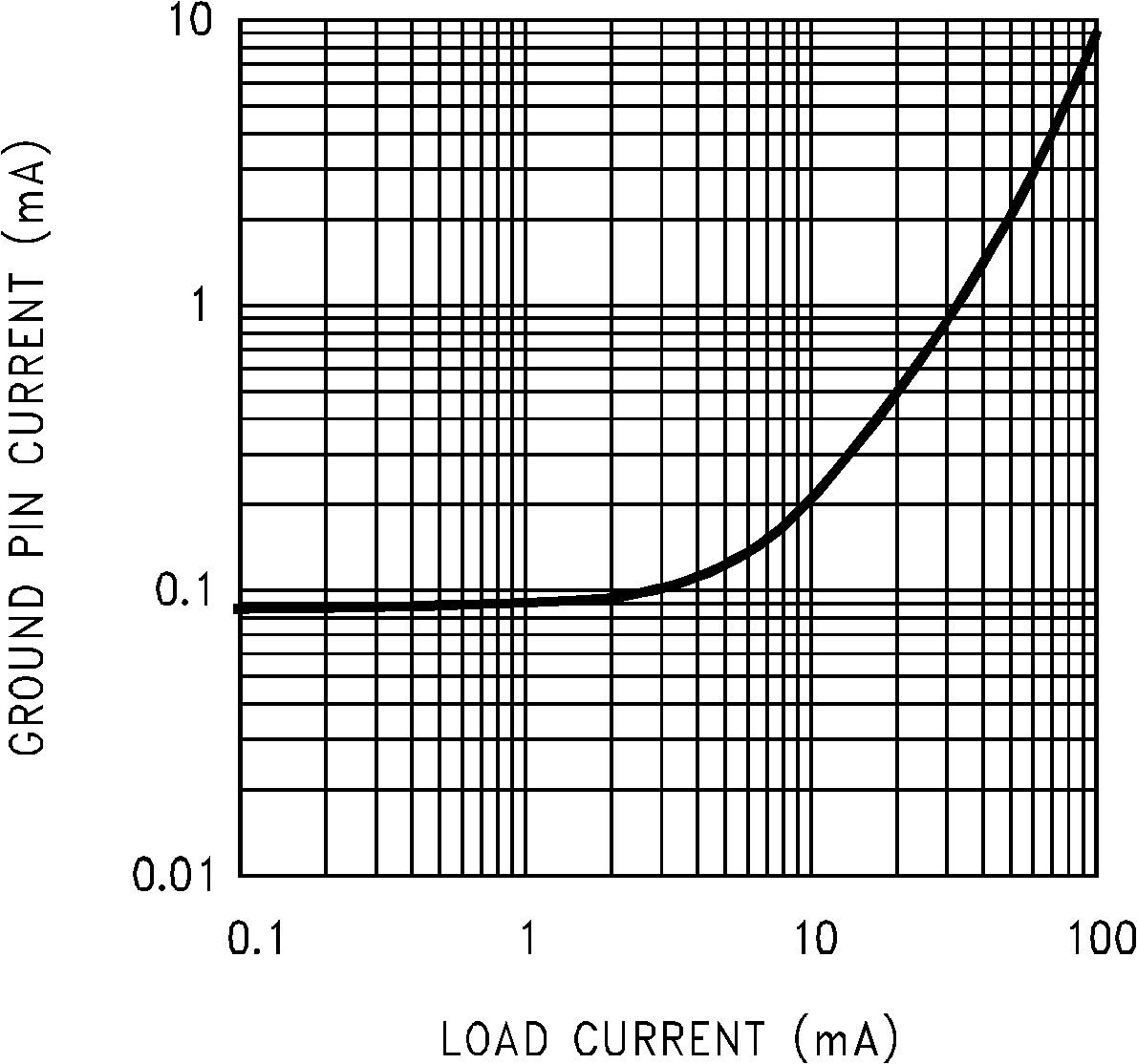 Figure 1. Quiescent Current
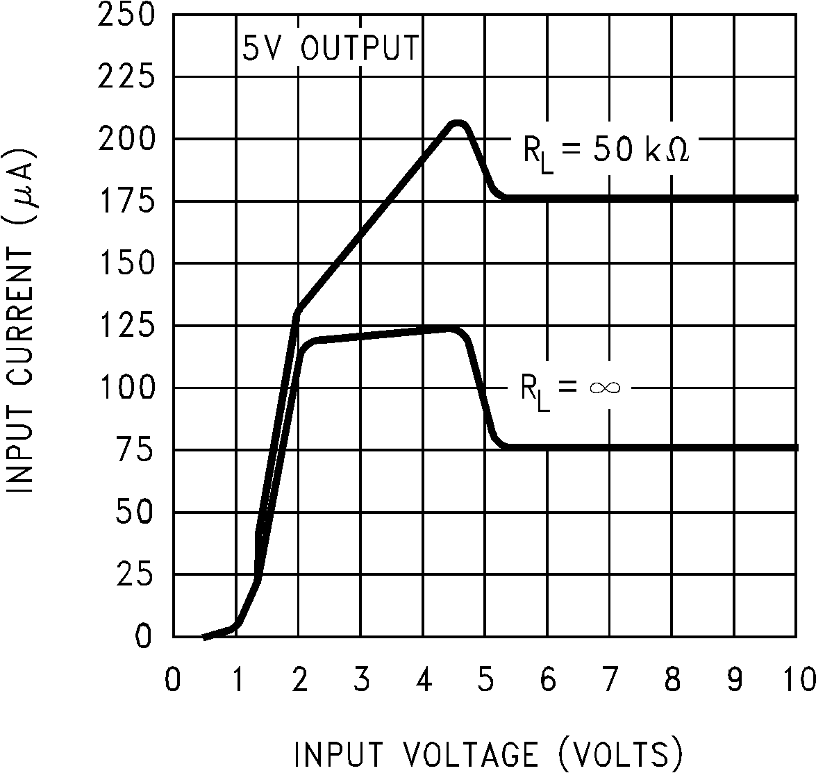 Figure 3. Input Current
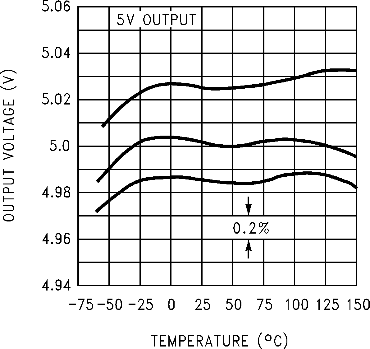 Figure 5. Output Voltage vs. Temperature of 3 Representative Units
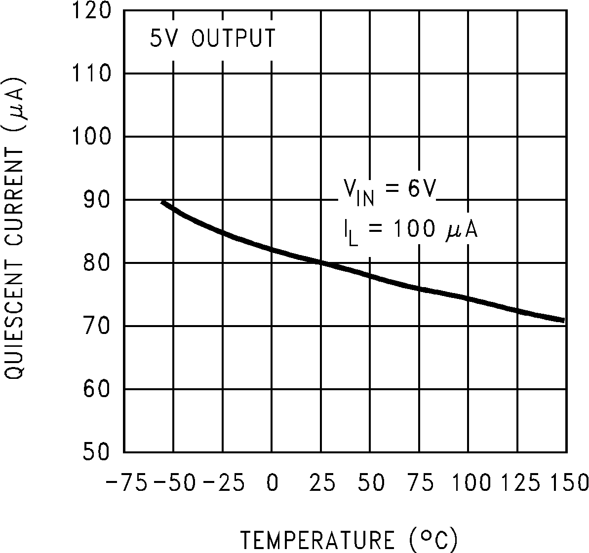 Figure 7. Quiescent Current
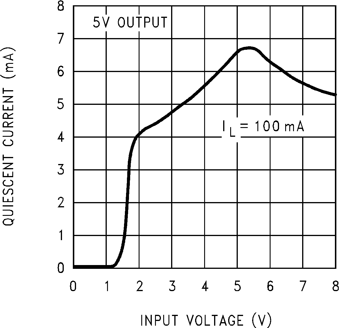 Figure 9. Quiescent Current
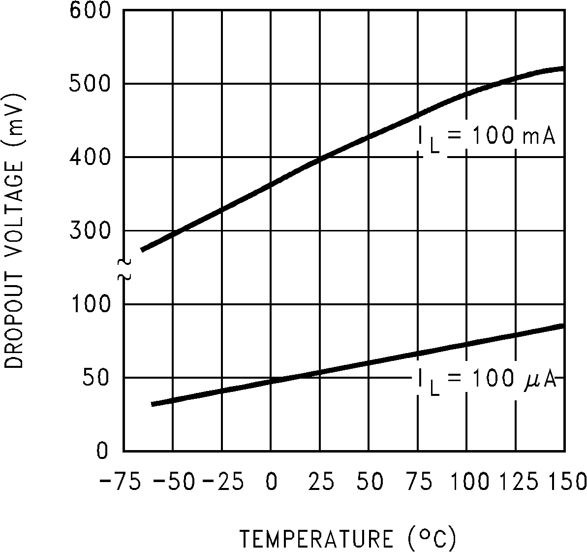 Figure 11. Dropout Voltage
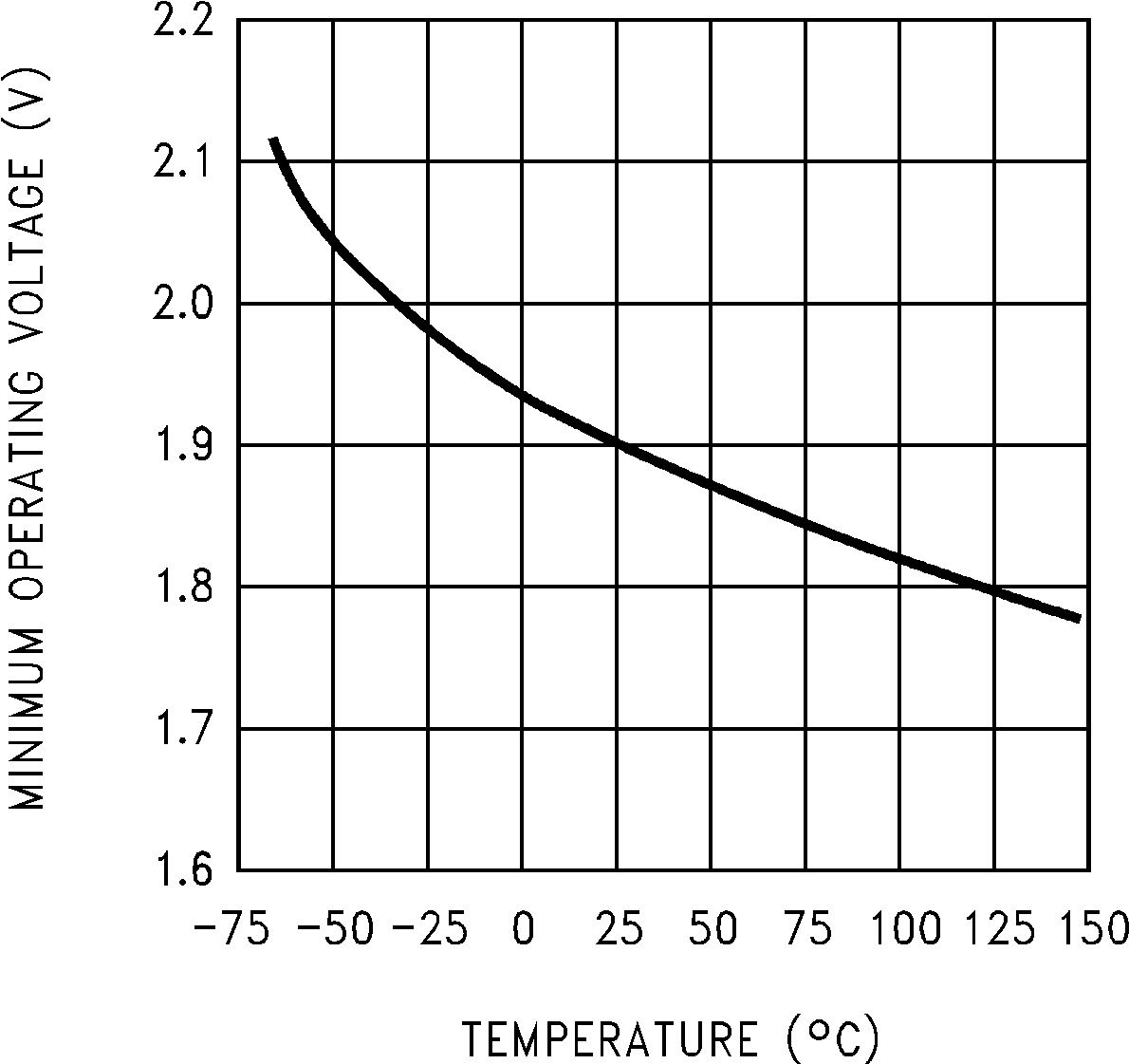 Figure 13. LP2951-N Minimum Operating Voltage
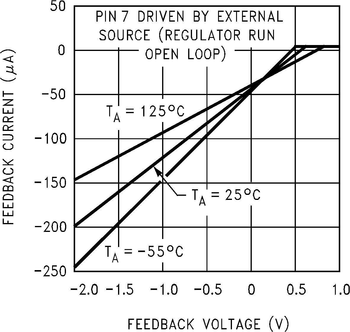 Figure 15. LP2951-N Feedback Pin Current
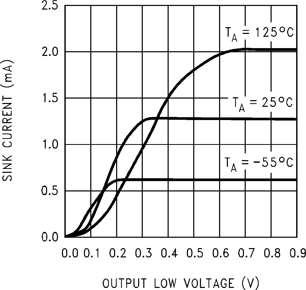 Figure 17. LP2951-N Comparator Sink Current
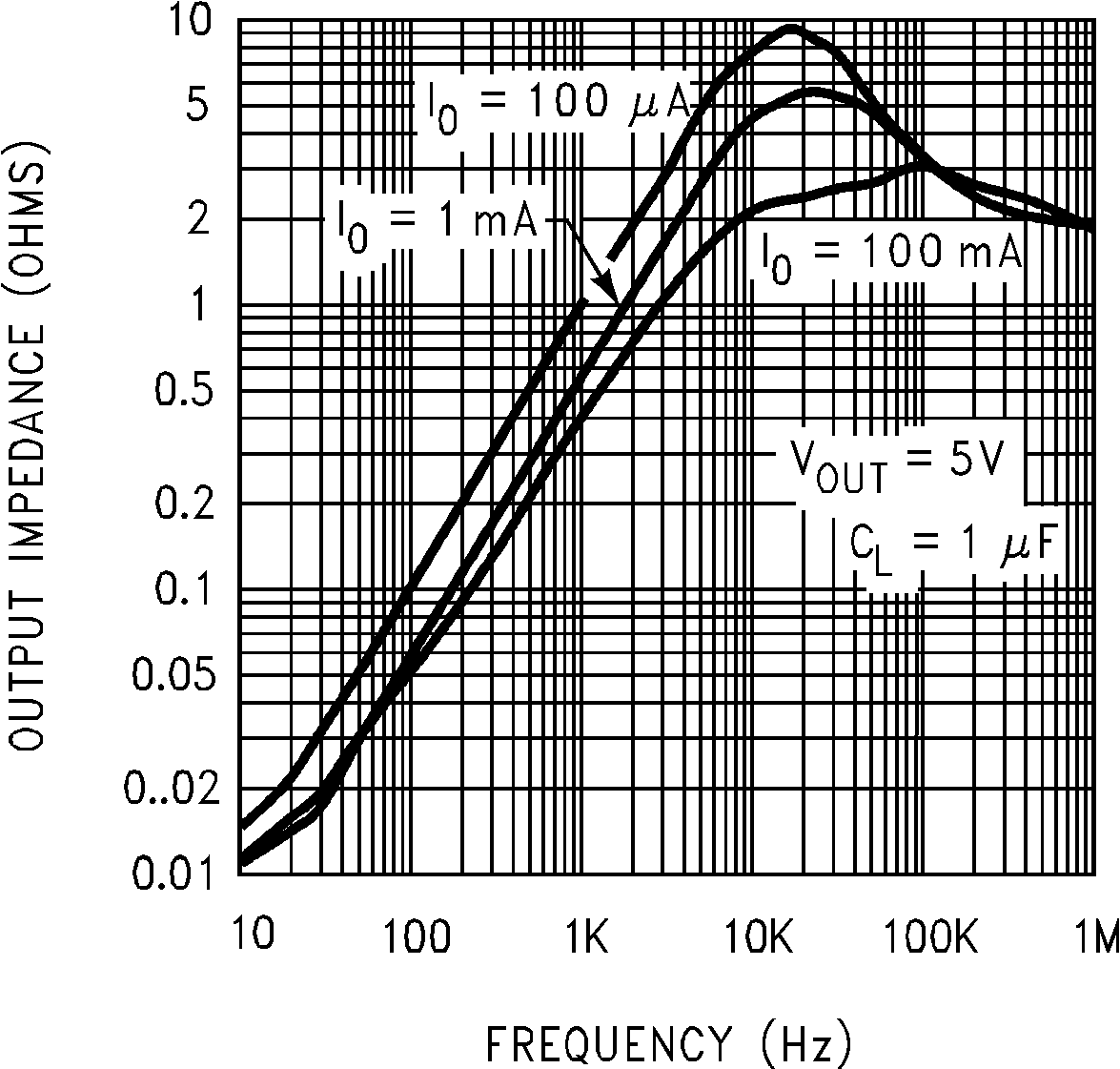 Figure 19. Output Impedance
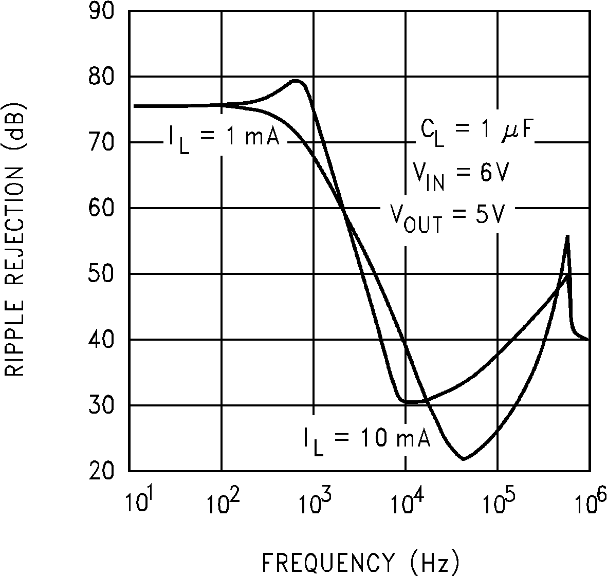 Figure 21. Ripple Rejection
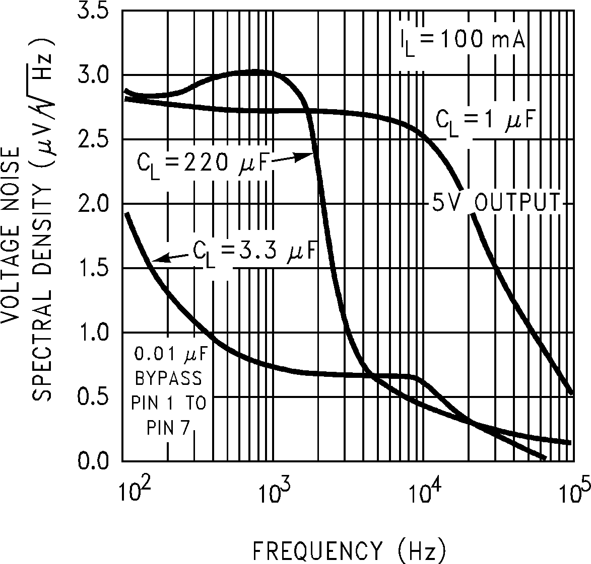 Figure 23. LP2951-N Output Noise
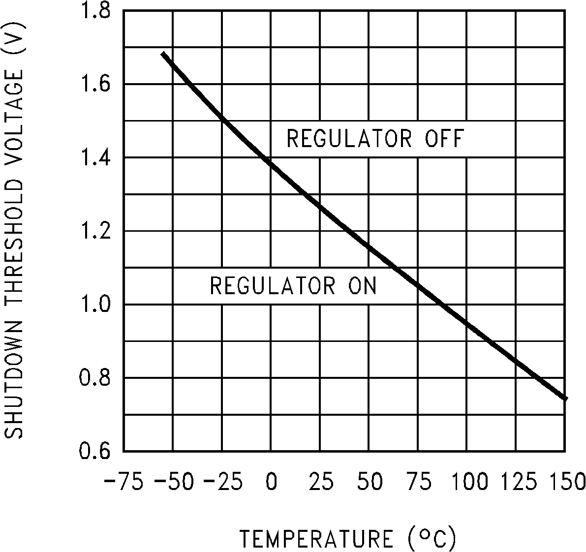 Figure 25. Shutdown Threshold Voltage
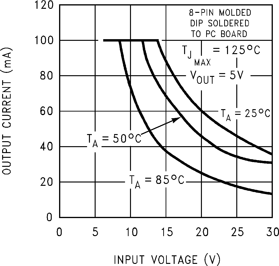 Figure 27. LP2951-N Maximum Rated Output Current
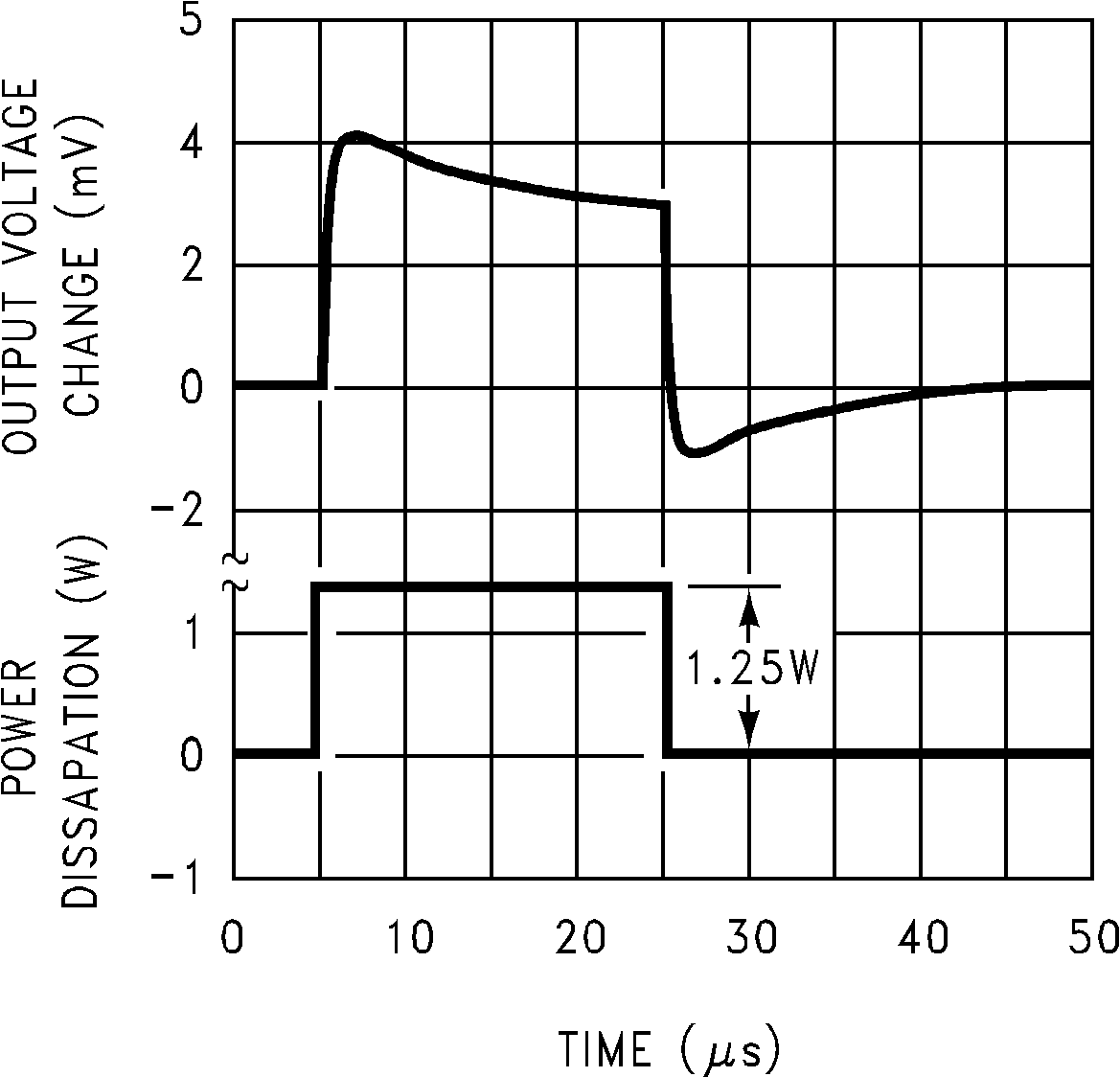 Figure 29. Thermal Response
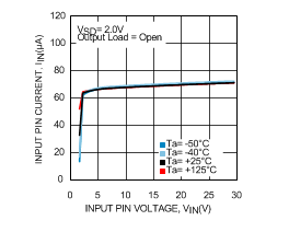 Figure 31. LP2951-N Input Pin Current vs Input Voltage
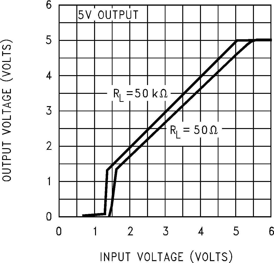 Figure 2. Dropout Characteristics
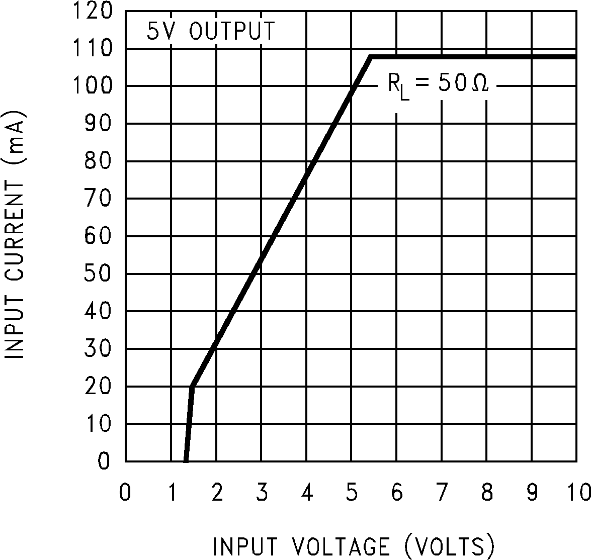 Figure 4. Input Current
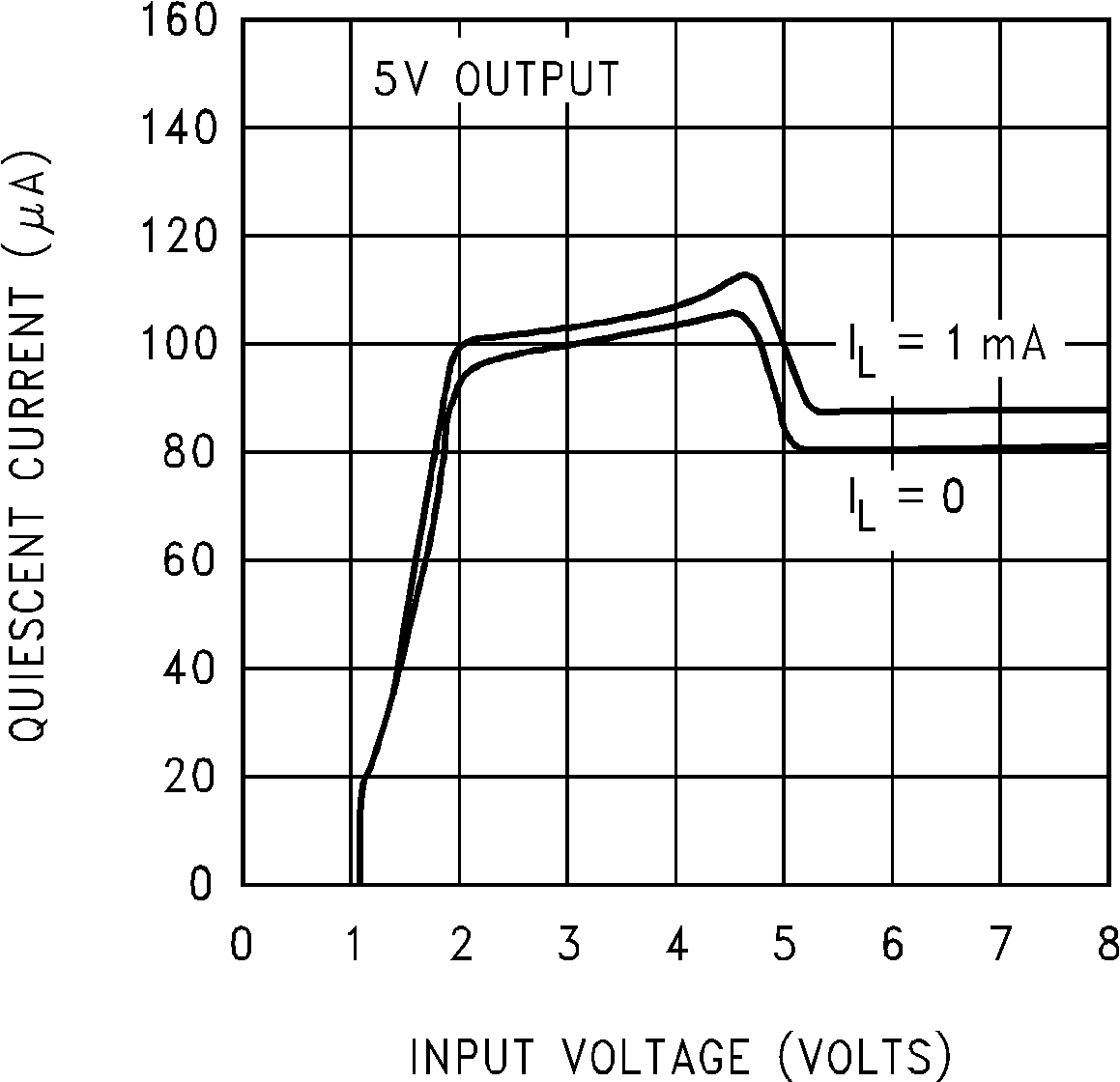 Figure 6. Quiescent Current
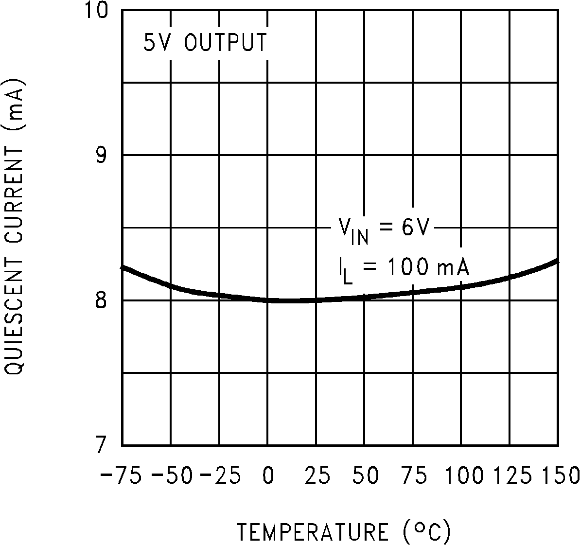 Figure 8. Quiescent Current
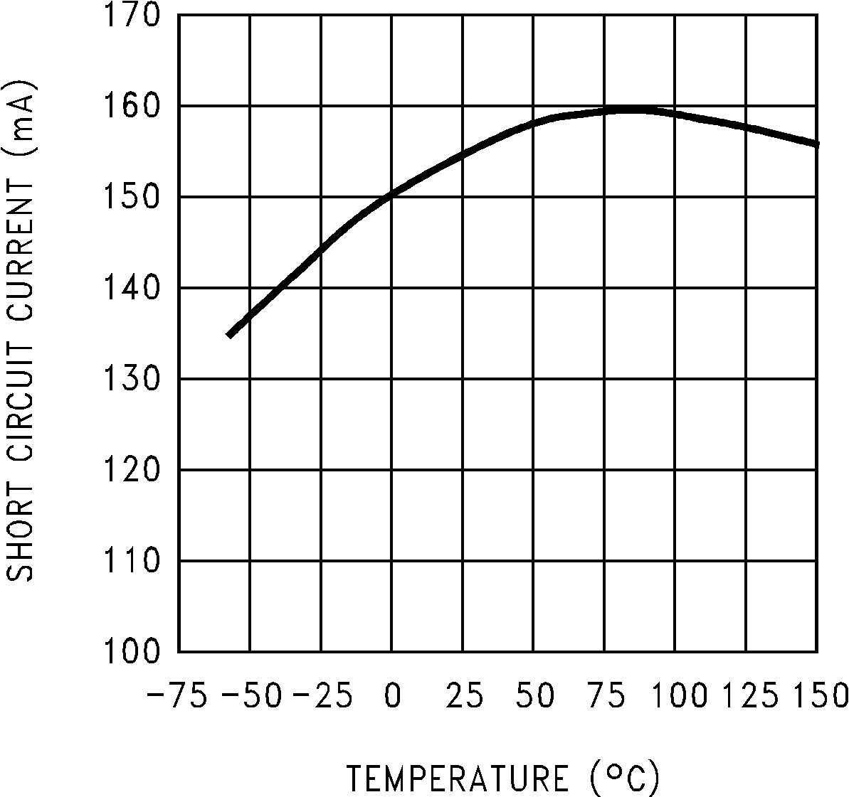 Figure 10. Short Circuit Current
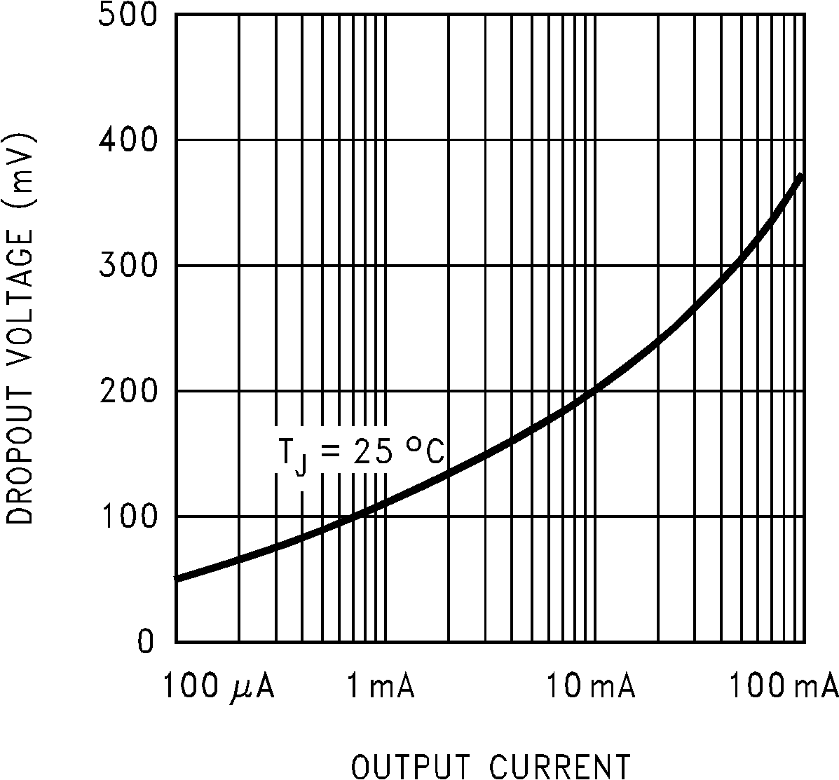 Figure 12. Dropout Voltage
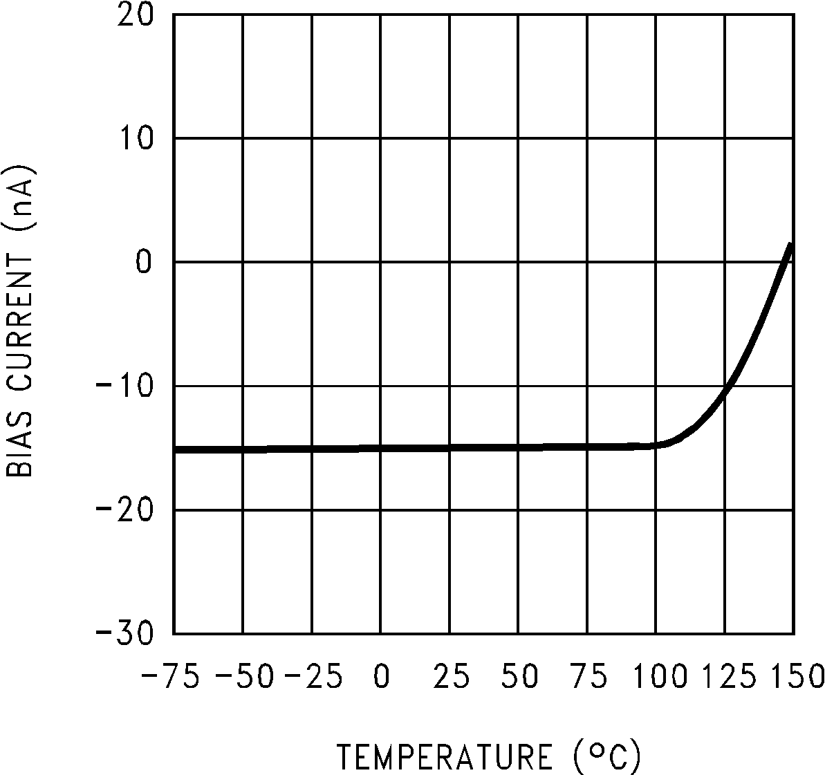 Figure 14. LP2951-N Feedback Bias Current
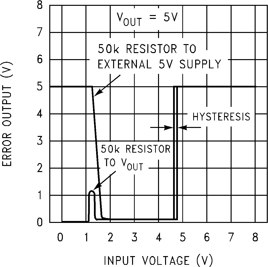 Figure 16. LP2951-N Error Comparator Output
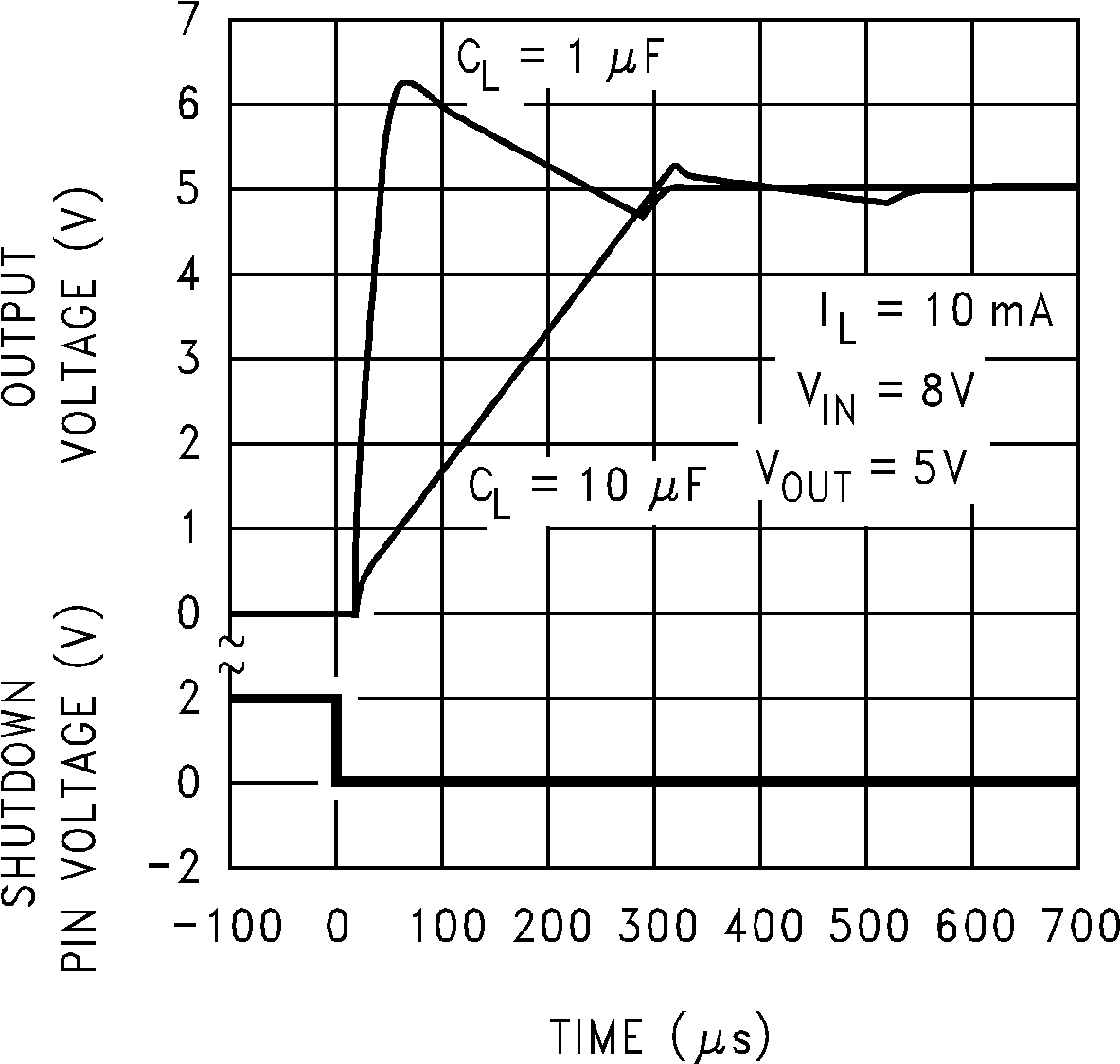 Figure 18. LP2951-N Enable Transient
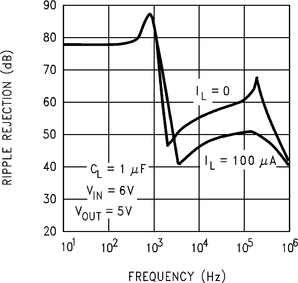 Figure 20. Ripple Rejection
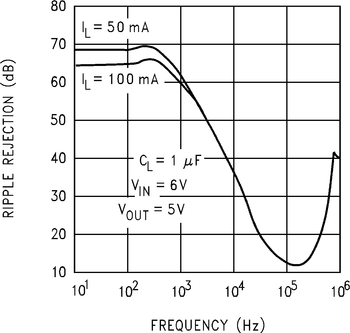 Figure 22. Ripple Rejection
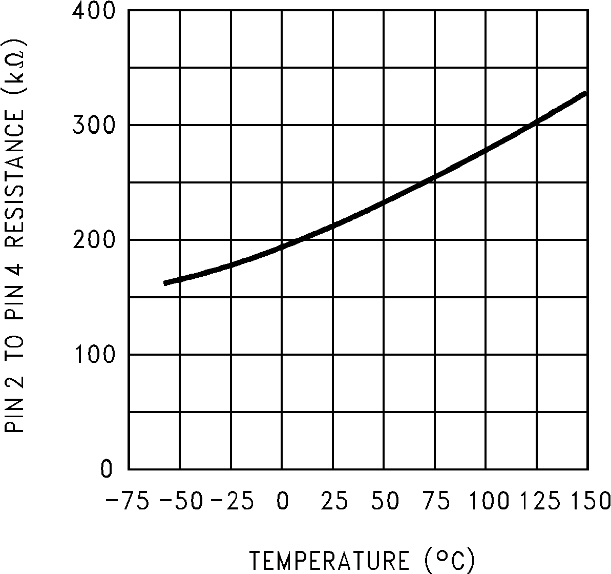 Figure 24. LP2951-N Divider Resistance
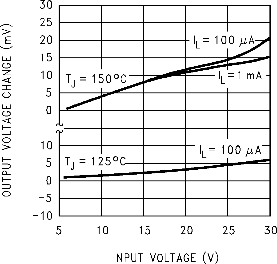 Figure 26. Line Regulation
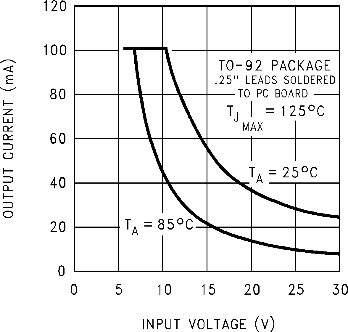 Figure 28. LP2950-N Maximum Rated Output Current
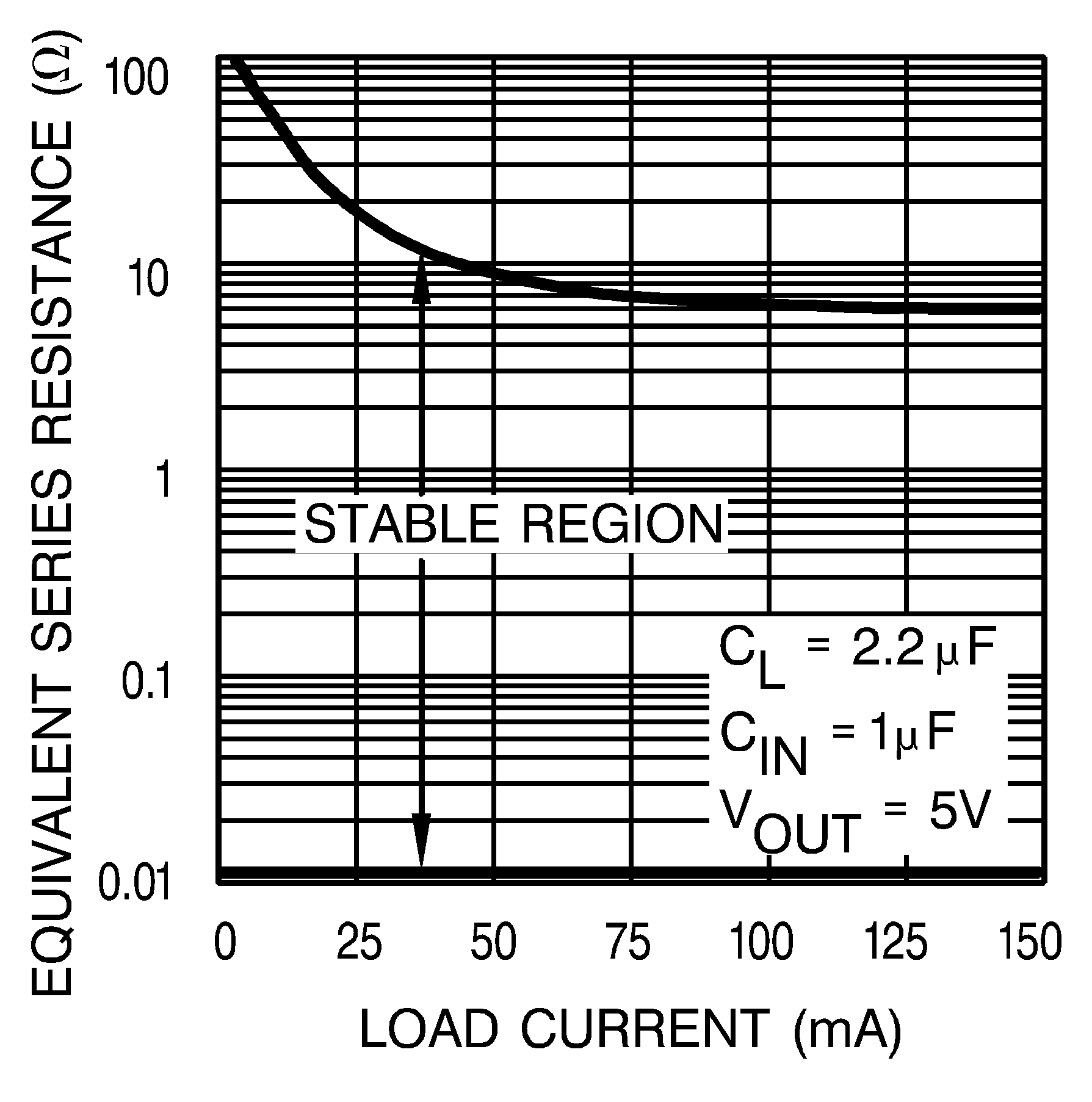 Figure 30. Output Capacitor ESR Range
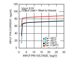 Figure 32. LP2951-N Input Pin Current vs Input Voltage