SLVS582J April   2006  – August 2024 LP2950 , LP2951

PRODUCTION DATA  

  1.   1
  2. Features
  3. Applications
  4. Description
  5. Pin Configuration and Functions
  6. Specifications
    1. 5.1 Absolute Maximum Ratings
    2. 5.2 ESD Ratings
    3. 5.3 Recommended Operating Conditions
    4. 5.4 Thermal Information
    5. 5.5 Electrical Characteristics (Both Legacy and New Chip)
    6. 5.6 Timing Requirements
    7. 5.7 Typical Characteristics
  7. Detailed Description
    1. 6.1 Overview
    2. 6.2 Functional Block Diagrams
    3. 6.3 Feature Description
      1. 6.3.1 Output Enable
      2. 6.3.2 Dropout Voltage
      3. 6.3.3 Current Limit
      4. 6.3.4 Undervoltage Lockout (UVLO)
      5. 6.3.5 Thermal Shutdown
    4. 6.4 Device Functional Modes
      1. 6.4.1 Shutdown Mode
  8. Application and Implementation
    1. 7.1 Application Information
      1. 7.1.1 Reverse Current
      2. 7.1.2 Input and Output Capacitor Requirements
      3. 7.1.3 Estimating Junction Temperature
      4. 7.1.4 Power Dissipation (PD)
    2. 7.2 Typical Application
      1. 7.2.1 Design Requirements
        1. 7.2.1.1 Recommended Capacitor Types
          1. 7.2.1.1.1 Recommended Capacitors for the Legacy Chip
          2. 7.2.1.1.2 Recommended Capacitors for the New Chip
      2. 7.2.2 Detailed Design Procedure
        1. 7.2.2.1 Feedback Resistor Selection
        2. 7.2.2.2 Feedforward Capacitor
      3. 7.2.3 Application Curve
    3. 7.3 Power Supply Recommendations
    4. 7.4 Layout
      1. 7.4.1 Layout Guidelines
      2. 7.4.2 Layout Example
  9. Device and Documentation Support
    1. 8.1 Device Support
      1. 8.1.1 Development Support
    2. 8.2 Receiving Notification of Documentation Updates
    3. 8.3 Device Nomenclature
    4. 8.4 Documentation Support
      1. 8.4.1 Related Documentation
    5. 8.5 Support Resources
    6. 8.6 Trademarks
    7. 8.7 Electrostatic Discharge Caution
    8. 8.8 Glossary
  10. Revision History
  11. 10Mechanical, Packaging, and Orderable Information

封装选项

机械数据 (封装 | 引脚)
散热焊盘机械数据 (封装 | 引脚)
订购信息

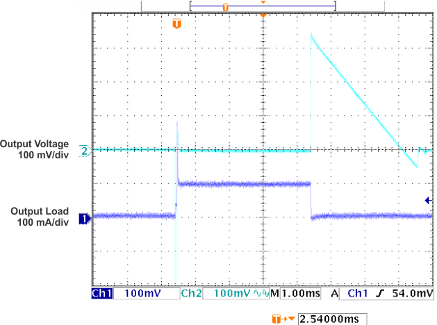
Application Curve

LP2950 LP2951 Load
                        Transient Response vs Time (VOUT = 5V, CL =
                        1µF)Figure 7-5 Load Transient Response vs Time (VOUT = 5V, CL = 1µF)