SNVS096E June 1999 – July 2016 LP2954 , LP2954A
PRODUCTION DATA.
- 1 Features
- 2 Applications
- 3 Description
- 4 Revision History
- 5 Pin Configuration and Functions
- 6 Specifications
- 7 Detailed Description
- 8 Application and Implementation
- 9 Power Supply Recommendations
- 10Layout
- 11Device and Documentation Support
- 12Mechanical, Packaging, and Orderable Information
封装选项
机械数据 (封装 | 引脚)
散热焊盘机械数据 (封装 | 引脚)
- KTT|3
订购信息
8 Application and Implementation
NOTE
Information in the following applications sections is not part of the TI component specification, and TI does not warrant its accuracy or completeness. TI’s customers are responsible for determining suitability of components for their purposes. Customers should validate and test their design implementation to confirm system functionality.
8.1 Application Information
The LP2954-N is a linear voltage regulator operating from 2.3 V to 30 V on the input and regulated output voltage of 5 V with typical 0.5% accuracy (LP2954AI) and 250 mA maximum output current. For linear voltage regulator the efficiency is defined by the ratio of output voltage to input voltage (efficiency = VOUT/VIN). To achieve high efficiency, the dropout voltage (VIN – VOUT) must be as small as possible, thus requiring a very low dropout LDO. Successfully implementing an LDO in an application depends on the application requirements. If the requirements are simply input voltage and output voltage, compliance specifications (such as internal power dissipation or stability) must be verified to ensure a solid design. If timing, start-up, noise, PSRR, or any other transient specification is required, the design becomes more challenging.
8.2 Typical Application
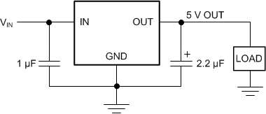 Figure 18. LP2954 Typical Application
8.2.1 Design Requirements
For typical LDO applications, use the parameters listed in Table 1.
Table 1. Design Parameters
| DESIGN PARAMETER | EXAMPLE VALUE |
|---|---|
| Input voltage | 2.5 V to 30 V |
| Output voltage | 1.23 V to 29 V |
| Output current | 250 mA (maximum) |
| RMS noise, 10 Hz to100 kHz | 260 μVRMS |
8.2.2 Detailed Design Procedure
8.2.2.1 External Capacitors
A 2.2 μF (or greater) capacitor is required between the OUT pin and GND to assure stability (refer to Figure 20). Without this capacitor, the device may oscillate. Most types of tantalum or aluminum electrolytic capacitors work here. Film-type capacitors work, but are more expensive. Many aluminum electrolytics contain electrolytes which freeze at −30°C, which requires the use of solid tantalums below −25°C. The important parameters of the capacitor are an equivalent series resistance (ESR) of about 5 Ω or less and a resonant frequency above 500 kHz (the ESR may increase by a factor of 20 or 30 as the temperature is reduced from 25°C to −30°C). The value of this capacitor may be increased without limit. At lower values of output current, less output capacitance is required for stability. The capacitor can be reduced to 0.68 μF for currents below 10 mA or 0.22 μF for currents below 1 mA.
Place a 1-μF capacitor from the IN pin to GND if there is more than 10 inches of wire between the input and the AC filter capacitor or if a battery input is used.
Programming the output for voltages below 5 V runs the error amplifier at lower gains requiring more output capacitance for stability. At 3.3-V output, a minimum of 4.7 μF is required. For the worst case condition of 1.23-V output and 250 mA of load current, a 6.8-μF (or larger) capacitor must be used.
Stray capacitance to the FEEDBACK pin can cause instability. This problem is most likely to appear when using high value external resistors to set the output voltage. Adding a 100-pF capacitor between the OUT and FEEDBACK pins and increasing the output capacitance to 6.8 μF (or greater) solves the problem.
8.2.2.2 Minimum Load
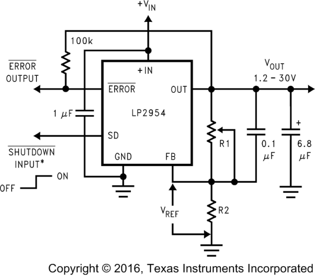
When setting the output voltage using an external resistive divider, TI recommends a minimum current of 1 μA through the resistors to provide a minimum load.
It should be noted that a minimum load current is specified in several of the electrical characteristic test conditions, so this value must be used to obtain correlation on these tested limits. The part is parametrically tested down to 100 μA, but is functional with no load.
8.2.2.3 Programming The Output Voltage
The SOIC version of the LP2954 regulator may be pin strapped for 5-V operation using its internal resistive divider by tying the OUT and SENSE pins together and also tying the FEEDBACK and 5V TAP pins together.
Alternatively, it may be programmed for any voltage between the 1.23-V reference and the 30-V maximum rating using an external pair of resistors (see Figure 19). The complete equation for the output voltage is:
where VREF is the 1.23-V reference and IFB is the FEEDBACK pin bias current (−20 nA typical). The minimum recommended load current of 1 μA sets an upper limit of 1.2 MΩ on the value of R2 in cases where the regulator must work with no load (see Minimum Load). IFB produces a typical 2% error in VOUT which can be eliminated at room temperature by trimming R1. For better accuracy, choosing R2 = 100 kΩ reduces this error to 0.17% while increasing the resistor program current to 12 μA. Because the typical quiescent current is 120 μA, this added current is negligible.
8.2.2.4 Power Dissipation
Knowing the device power dissipation and proper sizing of the thermal plane connected to the tab or pad is critical to ensuring reliable operation. Device power dissipation depends on input voltage, output voltage, and load conditions and can be calculated with Equation 3.
Power dissipation can be minimized, and greater efficiency can be achieved, by using the lowest available voltage drop option that would still be greater than the dropout voltage (VDO). However, keep in mind that higher voltage drops result in better dynamic (that is, PSRR and transient) performance.
Power dissipation and junction temperature are most often related by the junction-to-ambient thermal resistance (RθJA) of the combined PCB and device package and the temperature of the ambient air (TA), according to Equation 4 or Equation 5:
Unfortunately, this RθJA is highly dependent on the heat-spreading capability of the particular PCB design, and therefore varies according to the total copper area, copper weight, and location of the planes. The RθJA recorded in Thermal Information is determined by the specific EIA/JEDEC JESD51-7 standard for PCB and copper-spreading area, and is to be used only as a relative measure of package thermal performance. For a well-designed thermal layout, RθJA is actually the sum of the package junction-to-case (bottom) thermal resistance (RθJCbot) plus the thermal resistance contribution by the PCB copper area acting as a heat sink.
8.2.2.5 Estimating Junction Temperature
The EIA/JEDEC standard recommends the use of psi (Ψ) thermal characteristics to estimate the junction temperatures of surface mount devices on a typical PCB board application. These characteristics are not true thermal resistance values, but rather package specific thermal characteristics that offer practical and relative means of estimating junction temperatures. These psi metrics are determined to be significantly independent of copper-spreading area. The key thermal characteristics (ΨJT and ΨJB) are given in Thermal Information and are used in accordance with Equation 6 or Equation 7.
where
- PD(MAX) is explained in Equation 5
- TTOP is the temperature measured at the center-top of the device package.
where
- PD(MAX) is explained in Equation 5.
- TBOARD is the PCB surface temperature measured 1-mm from the device package and centered on the package edge.
For more information about the thermal characteristics ΨJT and ΨJB, Semiconductor and IC Package Thermal Metrics; for more information about measuring TTOP and TBOARD, see Using New Thermal Metrics; and for more information about the EIA/JEDEC JESD51 PCB used for validating RθJA, see Thermal Characteristics of Linear and Logic Packages Using JEDEC PCB Designs. These application notes are available at www.ti.com.
8.2.2.6 Heatsinking the TO-220 Package
A heat sink may be required with the LP2954IT depending on the maximum power dissipation and maximum ambient temperature of the application. Under all possible operating conditions, the junction temperature must be within the range specified under Recommended Operating Conditions.
To determine if a heat sink is required, the maximum power dissipated by the regulator, P(MAX), must be calculated. It is important to remember that if the regulator is powered from a transformer connected to the AC line, the maximum specified AC input voltage must be used (because this produces the maximum DC input voltage to the regulator). Figure 20 shows the voltages and currents that are present in the circuit. The formula for calculating the power dissipated in the regulator is also shown in Figure 20.
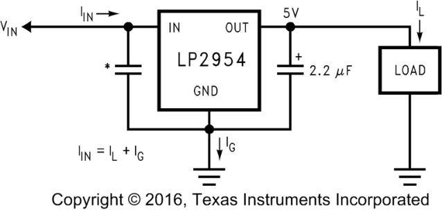 Figure 20. Basic 5-V Regulator Circuit
The next parameter which must be calculated is the maximum allowable temperature rise, TR(MAX). This is calculated by using the formula:
where
- TJ(MAX) is the maximum allowable junction temperature
- TA(MAX) is the maximum ambient temperature
Using the calculated values for TR(MAX) and P(MAX), the required value for junction-to-ambient thermal resistance, RθJA , can now be found:
If the calculated value is 60°C/W or higher , the regulator may be operated without an external heat sink. If the calculated value is below 60°C/W, an external heatsink is required. The required thermal resistance for this heat sink can be calculated using the formula:
where
- RθJC(bot) is the junction-to-case thermal resistance, which is specified as 0.9°C/W maximum for the LP2954IT
- RθCH is the case-to-heat-sink thermal resistance, which is dependent on the interfacing material (if used). For details and typical values in Table 2 and Table 3.
- Rθ(H-A) is the heatsink-to-ambient thermal resistance. It is this specification (listed on the heat-sink manufacturers data sheet) which defines the effectiveness of the heat sink. The heat sink selected must have a thermal resistance which is equal to or lower than the value of RθHA calculated from the above listed formula.
Table 2. Typical Values of Case-To-Heatsink Thermal Resistance (RθCH) (Data from Aavid Engineering)
| UNIT (C°/W) | |
| Silicone grease | 1 |
| Dry interface | 1.3 |
| Mica with grease | 1.4 |
Table 3. Typical Values Of Case-To-Heatsink Thermal Resistance (RθCH) (Data from Thermalloy)
| UNIT (C°/W) | |
| Thermasil III | 1.3 |
| Thermasil II | 1.5 |
| Thermalfilm (0.002) with grease | 2.2 |
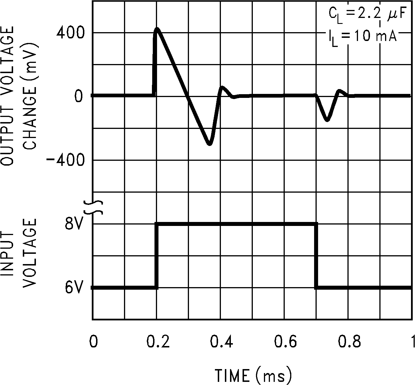
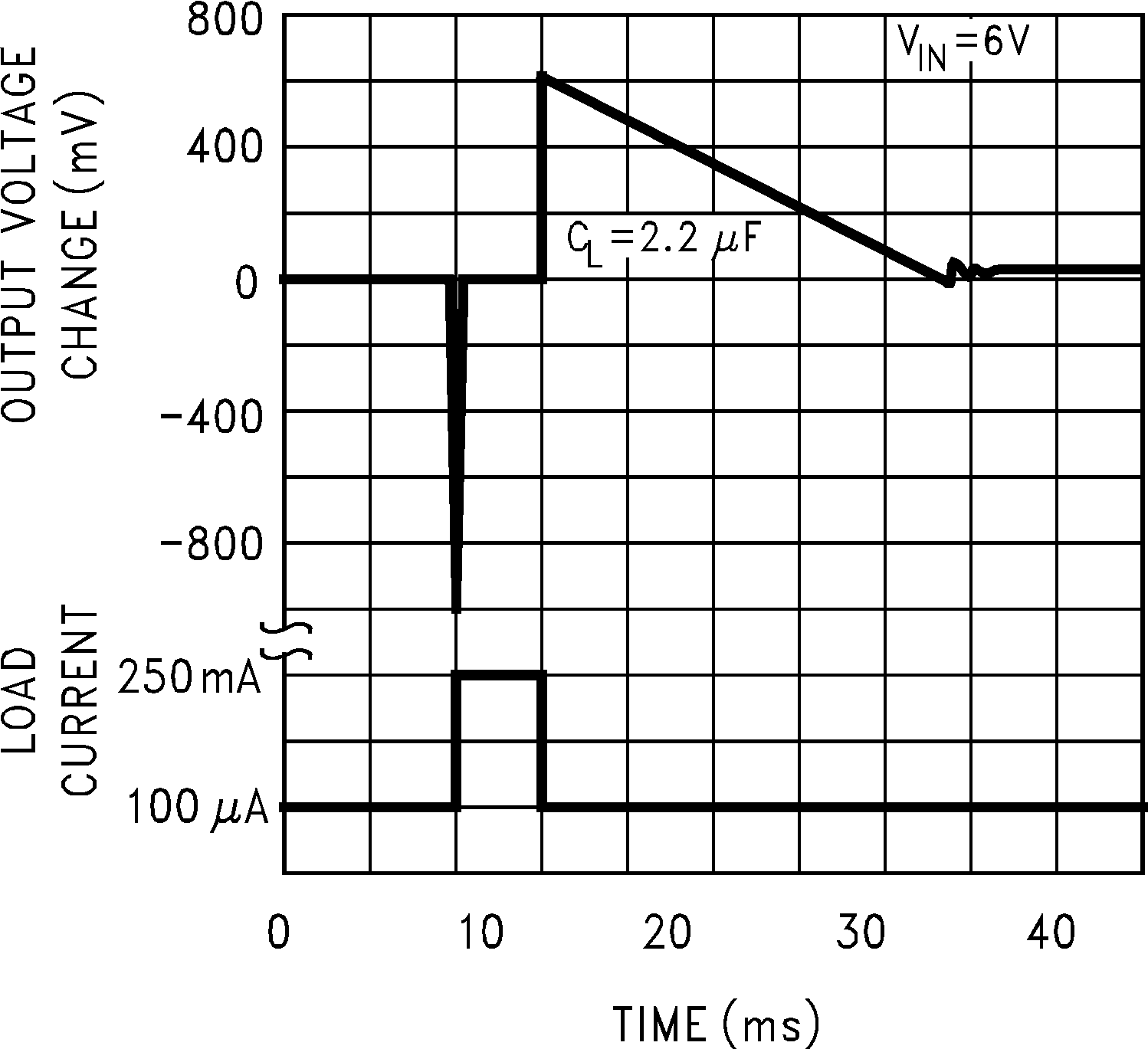
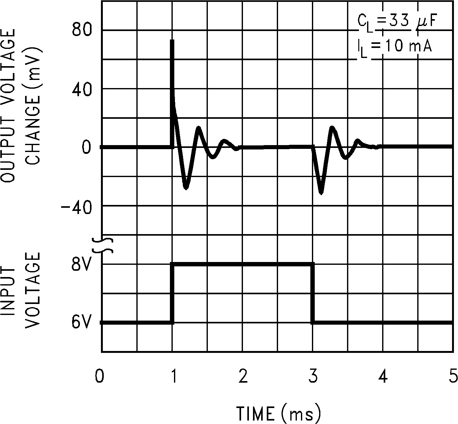
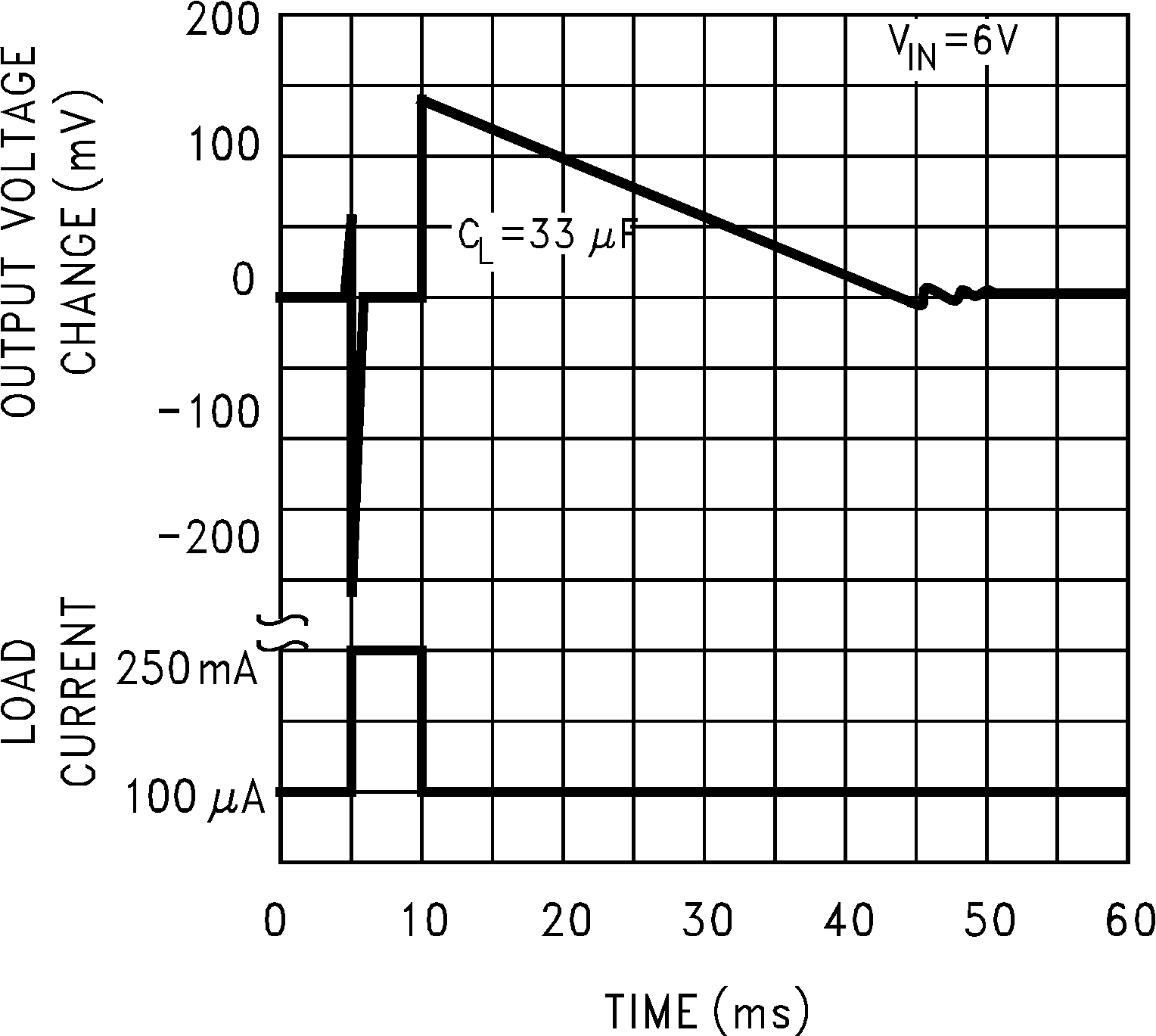
8.2.3 Application Curves
