SNVS096E June 1999 – July 2016 LP2954 , LP2954A
PRODUCTION DATA.
- 1 Features
- 2 Applications
- 3 Description
- 4 Revision History
- 5 Pin Configuration and Functions
- 6 Specifications
- 7 Detailed Description
- 8 Application and Implementation
- 9 Power Supply Recommendations
- 10Layout
- 11Device and Documentation Support
- 12Mechanical, Packaging, and Orderable Information
封装选项
机械数据 (封装 | 引脚)
散热焊盘机械数据 (封装 | 引脚)
- KTT|3
订购信息
7 Detailed Description
7.1 Overview
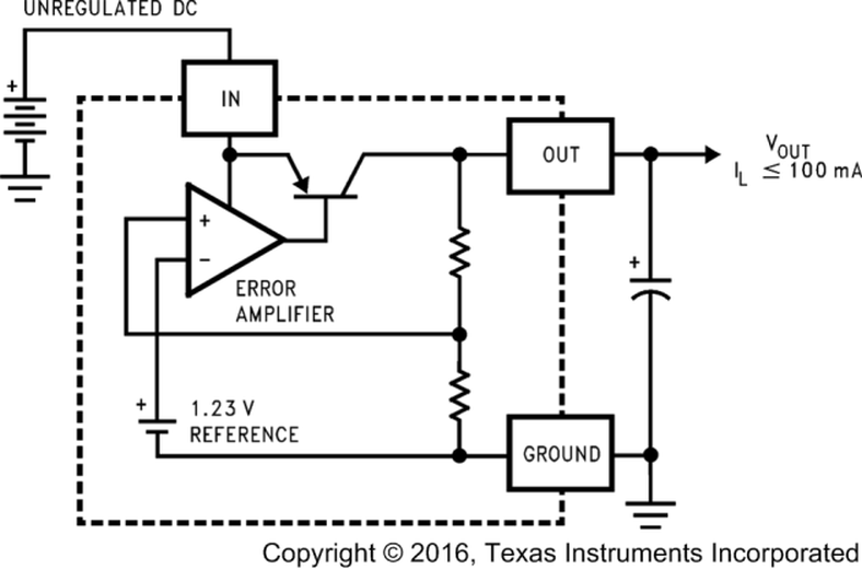
The LP2954 is a 5-V micropower LDO with very low quiescent current (90 μA typical at 1-mA load) and very low dropout voltage (typically 60 mV at light loads and 470 mV at 250-mA load current).
7.2 Functional Block Diagrams


7.3 Feature Description
7.3.1 Dropout Voltage
The dropout voltage of the regulator is defined as the minimum input-to-output voltage differential required for the output voltage to stay within 100 mV of the output voltage measured with a 1-V differential. The dropout voltages for various values of load current are listed under Electrical Characteristics.
If the regulator is powered from a rectified AC source with a capacitive filter, the minimum AC line voltage and maximum load current must be used to calculate the minimum voltage at the input of the regulator. The minimum input voltage, including AC ripple on the filter capacitor, must not drop below the voltage required to keep the LP2954 in regulation. It is also advisable to verify operating at minimum operating ambient temperature, because the increasing ESR of the filter capacitor makes this a worst-case test for dropout voltage due to increased ripple amplitude.
7.3.2 Dropout Detection Comparator
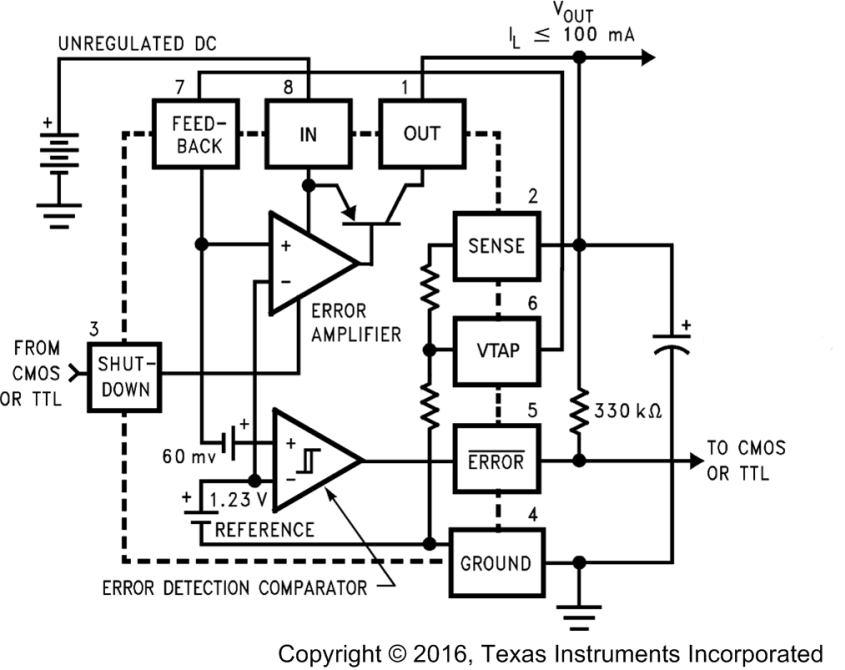
This comparator produces a logic LOW whenever the output falls out of regulation by more than about 5%. The 5% value is from the comparators built-in offset of 60 mV divided by the 1.23-V reference. The 5% low trip level remains constant regardless of the programmed output voltage. An out-of-regulation condition can result from low input voltage, current limiting, or thermal limiting.
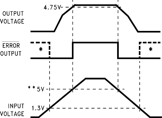
Figure 17 gives a timing diagram showing the relationship between the output voltage, the ERROR output, and input voltage as the input voltage is ramped up and down to a regulator programmed for 5-V output. The ERROR signal becomes low at about 1.3-V input. It goes high at about 5-V input, where the output equals 4.75 V. Because the dropout voltage is load dependent, the input voltage trip points vary with load current. The output voltage trip point does not vary.
The comparator has an open-collector output which requires an external pullup resistor. This resistor may be connected to the regulator output or some other supply voltage. Using the regulator output prevents an invalid HIGH on the comparator output which occurs if it is pulled up to an external voltage while the regulator input voltage is reduced below 1.3 V. In selecting a value for the pullup resistor note that, while the output can sink 400 μA, this current adds to battery drain. Suggested values range from 100 kΩ to 1 MΩ. This resistor is not required if the output is unused.
When VIN ≤ 1.3 V, the ERROR pin becomes a high impedance, allowing the error flag voltage to rise to its pullup voltage. Using VOUT as the pullup voltage (rather than an external 5-V source) keeps the error flag voltage below 1.2 V (typical) in this condition. The user may wish to divide down the error flag voltage using equal-value resistors (10 kΩ suggested) to ensure a low-level logic signal during any fault condition, while still allowing a valid high logic level during normal operation.

** Exact value depends on dropout voltage. (See Dropout Voltage)
7.3.3 Output Isolation
The regulator output can be left connected to an active voltage source (such as a battery) with the regulator input power turned off, as long as the regulator ground pin is connected to ground. If the ground pin is left floating, damage to the regulator can occur if the output is pulled up by an external voltage source.
7.3.4 Reducing Output Noise
In reference applications it may be advantageous to reduce the AC noise present on the output. One method is to reduce regulator bandwidth by increasing output capacitance. This is relatively inefficient, because large increases in capacitance are required to get significant improvement.
Noise can be reduced more effectively by a bypass capacitor placed across R1 (refer to Figure 19). The formula for selecting the capacitor to be used is:
This gives a value of about 0.1 μF. When this is used, the output capacitor must be 6.8 μF (or greater) to maintain stability. The 0.1-μF capacitor reduces the high frequency gain of the circuit to unity, lowering the output noise from 260 μV to 80 μV using a 10-Hz to 100-kHz bandwidth. Also, noise is no longer proportional to the output voltage, so improvements are more pronounced at high output voltages.
7.4 Device Functional Modes
7.4.1 Shutdown Input
A logic-level signal shuts off the regulator output when a LOW (< 1.2 V) is applied to the SHUTDOWN input.
To prevent possible mis-operation, the SHUTDOWN input must be actively terminated. If the input is driven from open-collector logic, a pullup resistor (TI recommends 20 kΩ to 100 kΩ) must be connected from the SHUTDOWN input to the regulator input.
If the SHUTDOWN input is driven from a source that actively pulls high and low (like an operational amplifier), the pullup resistor is not required, but may be used.
If the shutdown function is not to be used, the cost of the pullup resistor can be saved by simply tying the SHUTDOWN input directly to the regulator input.
IMPORTANT: Because the Absolute Maximum Ratings state that the SHUTDOWN input cannot go more than 0.3 V below ground, the reverse-battery protection feature that protects the regulator input is sacrificed if the SHUTDOWN input is tied directly to the regulator input.
If reverse-battery protection is required in an application, the pullup resistor between the SHUTDOWN input and the regulator input must be used. The recommended 20 kΩ to 100 kΩ provides adequate protection of the SHUTDOWN pin during negative voltage transitions at the IN pin.