SNVS096E June 1999 – July 2016 LP2954 , LP2954A
PRODUCTION DATA.
- 1 Features
- 2 Applications
- 3 Description
- 4 Revision History
- 5 Pin Configuration and Functions
- 6 Specifications
- 7 Detailed Description
- 8 Application and Implementation
- 9 Power Supply Recommendations
- 10Layout
- 11Device and Documentation Support
- 12Mechanical, Packaging, and Orderable Information
封装选项
机械数据 (封装 | 引脚)
散热焊盘机械数据 (封装 | 引脚)
- KTT|3
订购信息
5 Pin Configuration and Functions
NDE Package
3-Pin TO-220
Front View

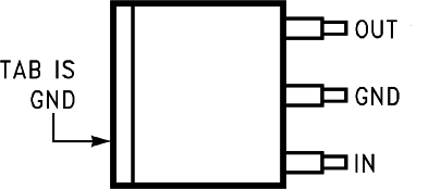
KTT Package
3-Pin DDPAK/TO-263
Front View

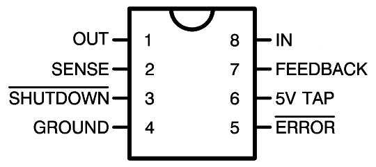
D Package
8-Pin SOIC
Top

Pin Functions
| PIN | I/O | DESCRIPTION | |||
|---|---|---|---|---|---|
| NAME | NDE | KTT | D | ||
| ERROR | — | — | 5 | O | Error output |
| FEEDBACK | — | — | 7 | I | Voltage feedback input |
| IN | 1 | 1 | 8 | I | Unregulated input voltage |
| GND | 2 | 2 | 4 | — | Ground |
| OUT | 3 | 3 | 1 | O | Regulated output voltage. This pin requires an output capacitor to maintain stability. See Detailed Design Procedure for output capacitor details |
| SENSE | — | — | 2 | I | Output voltage sense |
| SHUTDOWN | — | — | 3 | I | Disable device |
| 5V TAP | — | — | 6 | O | Internal resistor divider |