ZHCSU09H July   2004  – December 2023 LP2981 , LP2981A

PRODUCTION DATA  

  1.   1
  2. 特性
  3. 应用
  4. 说明
  5. Pin Configuration and Functions
  6. Specifications
    1. 5.1 Absolute Maximum Ratings
    2. 5.2 ESD Ratings
    3. 5.3 Recommended Operating Conditions
    4. 5.4 Thermal Information
    5. 5.5 Electrical Characteristics
    6. 5.6 Typical Characteristics
  7. Detailed Description
    1. 6.1 Overview
    2. 6.2 Functional Block Diagram
    3. 6.3 Feature Description
      1. 6.3.1 Output Enable
      2. 6.3.2 Dropout Voltage
      3. 6.3.3 Current Limit
      4. 6.3.4 Undervoltage Lockout (UVLO)
      5. 6.3.5 Thermal Shutdown
      6. 6.3.6 Output Pulldown
    4. 6.4 Device Functional Modes
      1. 6.4.1 Device Functional Mode Comparison
      2. 6.4.2 Normal Operation
      3. 6.4.3 Dropout Operation
      4. 6.4.4 Disabled
  8. Application and Implementation
    1. 7.1 Application Information
      1. 7.1.1 Recommended Capacitor Types
        1. 7.1.1.1 Recommended Capacitors for the Legacy Chip
          1. 7.1.1.1.1 Tantalum Capacitors
          2. 7.1.1.1.2 Ceramic Capacitors
          3. 7.1.1.1.3 Aluminum Capacitors
        2. 7.1.1.2 Recommended Capacitors for the New Chip
      2. 7.1.2 Input and Output Capacitor Requirements
        1. 7.1.2.1 Input Capacitor
        2. 7.1.2.2 Output Capacitor
      3. 7.1.3 Estimating Junction Temperature
      4. 7.1.4 Power Dissipation (PD)
      5. 7.1.5 Reverse Current
    2. 7.2 Typical Application
      1. 7.2.1 Design Requirements
      2. 7.2.2 Detailed Design Procedure
        1. 7.2.2.1 ON and OFF Input Operation
      3. 7.2.3 Application Curves
  9. Power Supply Recommendations
  10. Layout
    1. 9.1 Layout Guidelines
    2. 9.2 Layout Example
  11. 10Device and Documentation Support
    1. 10.1 Device Nomenclature
    2. 10.2 Documentation Support
      1. 10.2.1 Related Documentation
    3. 10.3 Receiving Notification of Documentation Updates
    4. 10.4 支持资源
    5. 10.5 Trademarks
    6. 10.6 静电放电警告
    7. 10.7 术语表
  12. 11Revision History
  13. 12Mechanical, Packaging, and Orderable Information

封装选项

机械数据 (封装 | 引脚)
散热焊盘机械数据 (封装 | 引脚)
订购信息

Application Curves

GUID-DCAEA379-7C45-4F7A-9A7E-53FA16B4D0C0-low.png
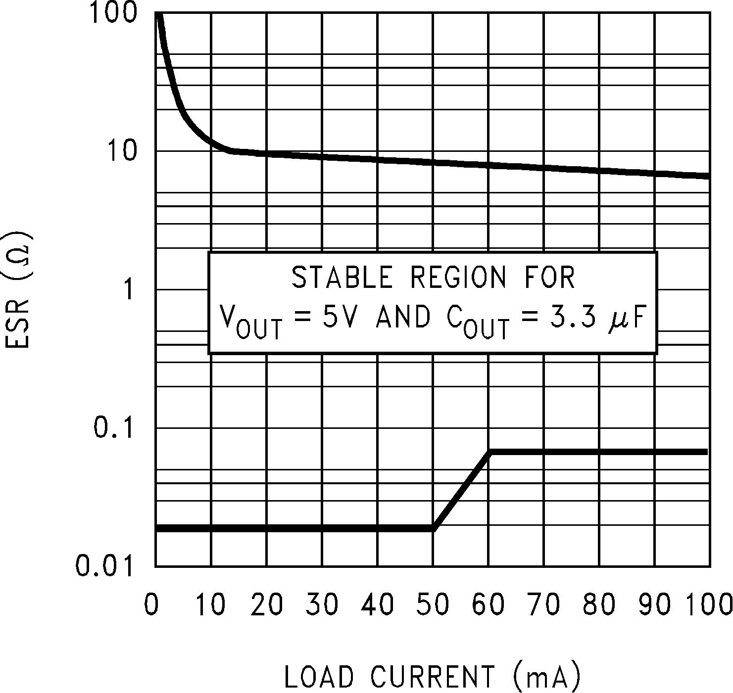
VOUT = 5 V, COUT = 3.3 μF
Figure 7-3 5-V, 3.3-μF ESR Curves (Legacy Chip)
GUID-ADE83CE3-C7D3-4E18-A7E1-C3B68C006F08-low.png
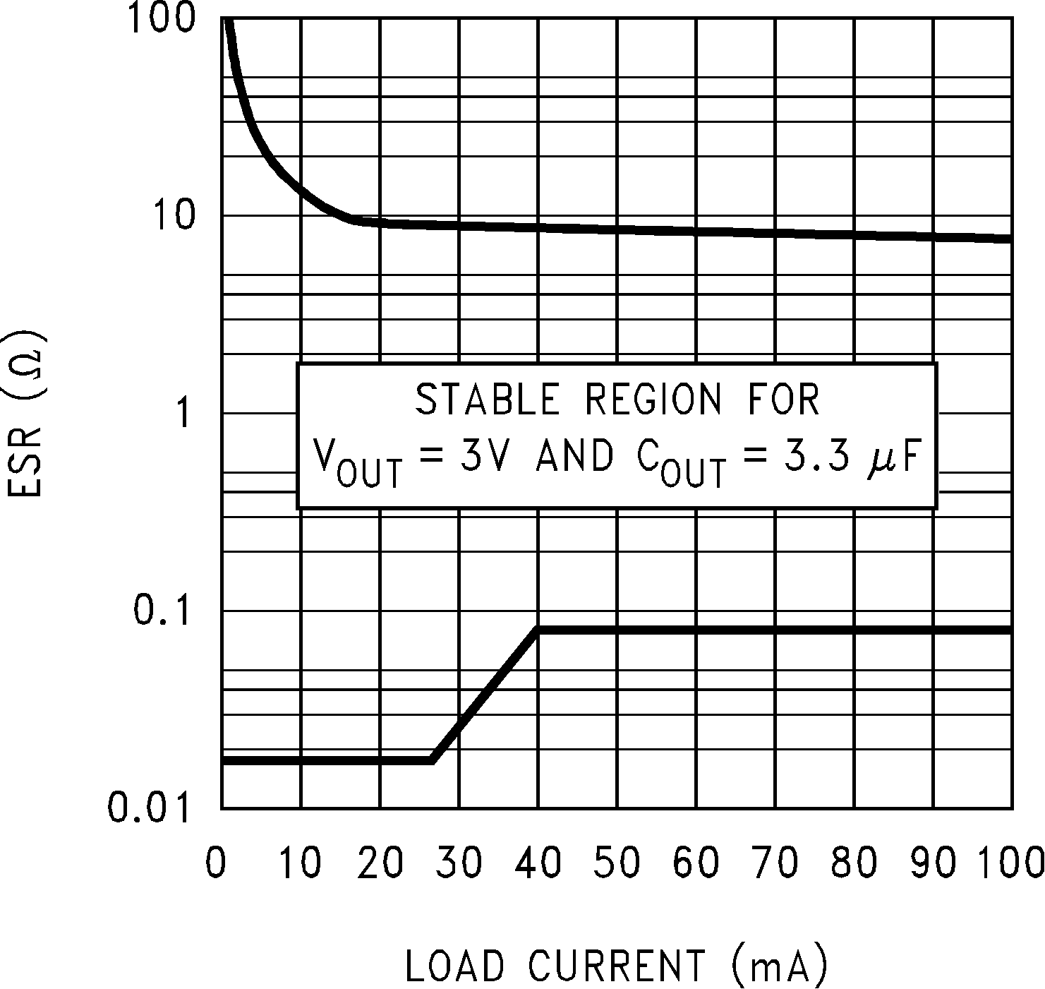
VOUT = 3.0 V, COUT = 3.3 μF
Figure 7-5 3.0-V, 3.3-μF ESR Curves (Legacy Chip)
GUID-20231203-SS0I-SX1H-KLJ1-WKBNBDFXK7J9-low.svg
VOUT = 3.3 V, IL = 100 mA
Figure 7-7 Line Transient Response (New Chip)
GUID-20231125-SS0I-9RVB-XJLQ-43DK3B88T3LM-low.svg
VOUT = 3.3 V, COUT = 2.2 μF
Figure 7-9 Load Transient Response (New Chip)
GUID-20231203-SS0I-2MBB-KD6J-XNSCBWRFWGRC-low.svg
VOUT = 5 V, RL = 5 kΩ
Figure 7-11 Turn-off Waveform (New Chip)
GUID-E9B65ACA-AEDB-4EDB-BC22-4A47447F1622-low.png
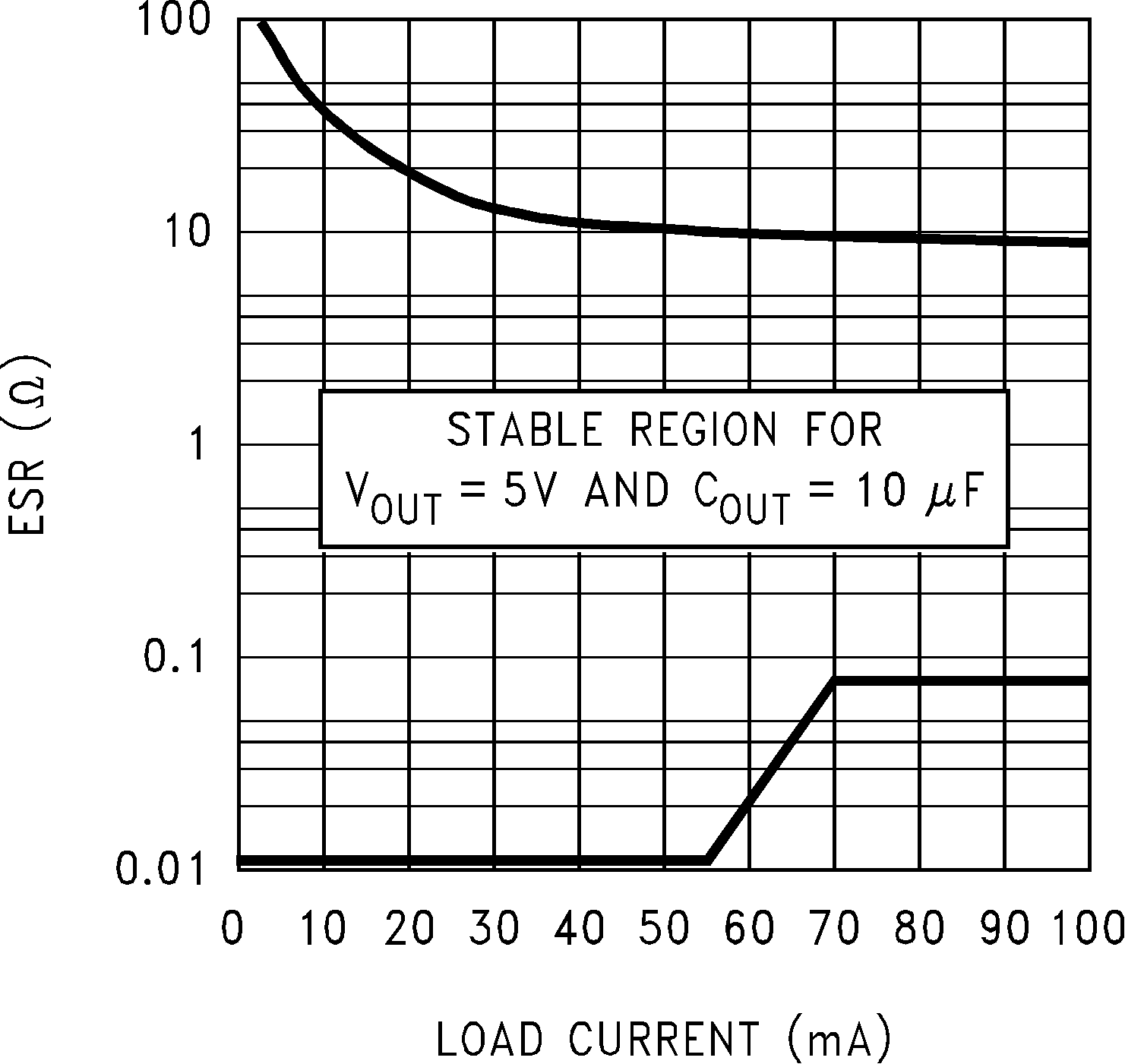
VOUT = 5 V, CL = 10 μF
Figure 7-4 5-V, 10-μF ESR Curves (Legacy Chip)
GUID-1F6D2BF5-F8C7-4F28-889E-11C45520B62F-low.png
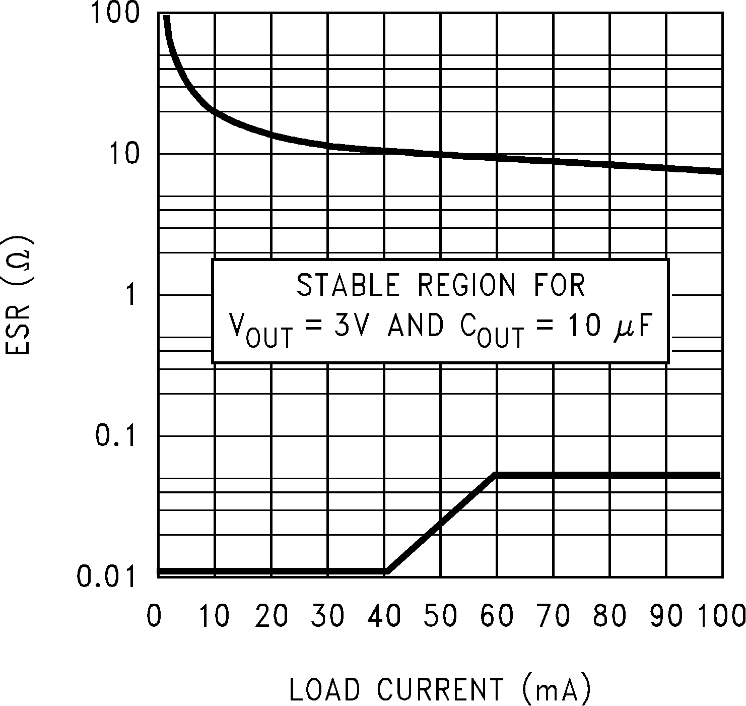
VOUT = 3.0 V, CL = 10 μF
Figure 7-6 3.0-V, 10-μF ESR Curves (Legacy Chip)
GUID-20231203-SS0I-WTMH-J9VM-P3BW6DMJJ48C-low.svg
VOUT = 3.3 V, IL = 1 mA
Figure 7-8 Line Transient Response (New Chip)
GUID-20231125-SS0I-37DK-VDB0-LKN3QRVMTSLL-low.svg
VOUT = 3.3 V, RL = 3.3 kΩ
Figure 7-10 Turn-on Waveform (New Chip)