SNVS137I March 1999 – September 2015 LP2986
PRODUCTION DATA.
- 1 Features
- 2 Applications
- 3 Description
- 4 Revision History
- 5 Pin Configuration and Function
- 6 Specifications
- 7 Detailed Description
- 8 Application and Implementation
- 9 Power Supply Recommendations
- 10Layout
- 11Device and Documentation Support
- 12Mechanical, Packaging, and Orderable Information
封装选项
机械数据 (封装 | 引脚)
散热焊盘机械数据 (封装 | 引脚)
订购信息
10 Layout
10.1 Layout Guidelines
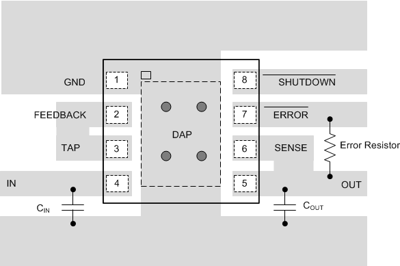
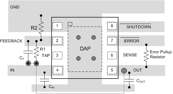
For best overall performance, place all circuit components on the same side of the circuit board and as near as practical to the respective LDO pin connections. Place ground return connections to the input and output capacitor, and to the LDO ground pin as close to each other as possible, connected by a wide, component-side, copper surface. The use of vias and long traces to create LDO circuit connections is strongly discouraged and negatively affects system performance. This grounding and layout scheme minimizes inductive parasitics, and thereby reduces load-current transients, minimizes noise, and increases circuit stability. A ground reference plane is also recommended and is either embedded in the PCB itself or located on the bottom side of the PCB opposite the components. This reference plane serves to assure accuracy of the output voltage, shield noise, and behaves similar to a thermal plane to spread (or sink) heat from the LDO device. In most applications, this ground plane is necessary to meet thermal requirements.
10.2 Layout Examples
 Figure 39. WSON Layout with Internal Resistor Divider
 Figure 40. WSON Layout with External Resistor Divider
10.3 WSON Mounting
The LDC08A (pullback) 8-pin WSON package requires specific mounting techniques which are detailed in Texas Instruments Application Note Leadless Leadframe Package (LLP) (SNOA401). Referring to the section PCB Design Recommendations in SNOA401, the pad style which should be used with this WSON package is the NSMD (non-solder mask defined) type. Additionally, for optimal reliability, there is a recommended 1:1 ratio between the package pad and the PCB pad for the pullback WSON.
The thermal dissipation of the WSON package is directly related to the printed circuit board construction and the amount of additional copper area connected to the DAP.
The DAP (exposed pad) on the bottom of the WSON package is connected to the die substrate with a conductive die attach adhesive. The DAP has no direct electrical (wire) connection to any of the eight pins. There is a parasitic PN junction between the die substrate and the device ground. As such, it is strongly recommend that the DAP be connected directly to the ground at device pin 1 (GROUND). Alternately, but not recommended, the DAP may be left floating (that is, no electrical connection). The DAP must not be connected to any potential other than ground.
For the LP2986 in the NGN 8-pin WSON package, the junction-to-case thermal rating (RθJC) is 4.4°C/W, where the case is on the bottom of the package at the center of the DAP.