SNVS137I March 1999 – September 2015 LP2986
PRODUCTION DATA.
- 1 Features
- 2 Applications
- 3 Description
- 4 Revision History
- 5 Pin Configuration and Function
- 6 Specifications
- 7 Detailed Description
- 8 Application and Implementation
- 9 Power Supply Recommendations
- 10Layout
- 11Device and Documentation Support
- 12Mechanical, Packaging, and Orderable Information
封装选项
机械数据 (封装 | 引脚)
散热焊盘机械数据 (封装 | 引脚)
订购信息
6 Specifications
6.1 Absolute Maximum Ratings
over operating free-air temperature range (unless otherwise noted)(1)(2)| MIN | MAX | UNIT | ||
|---|---|---|---|---|
| Input supply voltage (survival) | –0.3 | 16 | V | |
| Input supply voltage (operating) | 2.1 | 16 | V | |
| SHUTDOWN pin | –0.3 | 16 | V | |
| FEEDBACK pin | –0.3 | 5 | V | |
| Output voltage (survival)(3) | –0.3 | 16 | V | |
| IOUT (survival) | Short-circuit protected | |||
| Input-output voltage (survival)(4) | –0.3 | 16 | V | |
| Power dissipation(5) | Internally limited | |||
| Storage temperature, Tstg | −65 | 150 | °C | |
(1) Stresses beyond those listed under Absolute Maximum Ratings may cause permanent damage to the device. These are stress ratings only, which do not imply functional operation of the device at these or any other conditions beyond those indicated under Recommended Operating Conditions. Exposure to absolute-maximum-rated conditions for extended periods may affect device reliability.
(2) If Military/Aerospace specified devices are required, contact the Texas Instruments Sales Office/Distributors for availability and specifications.
(3) If used in a dual-supply system where the regulator load is returned to a negative supply, the LM2986 output must be diode-clamped to ground.
(4) The output PNP structure contains a diode between the IN and OUT pins that is normally reverse-biased. Forcing the output above the input will turn on this diode and may induce a latch-up mode which can damage the part (see Reverse Input-Output Voltage).
(5) The maximum allowable power dissipation is a function of the maximum junction temperature, TJ(MAX), the junction-to-ambient thermal resistance, RθJA, and the ambient temperature, TA. The maximum allowable power dissipation at any ambient temperature is calculated using: P(MAX) = TJ(MAX) – TA / RθJA
For improved thermal resistance and power dissipation for the WSON package, refer to Texas Instruments Application Note Leadless Leadframe Package (LLP) (SNOA401). Exceeding the maximum allowable power dissipation will cause excessive die temperature, and the regulator will go into thermal shutdown.
For improved thermal resistance and power dissipation for the WSON package, refer to Texas Instruments Application Note Leadless Leadframe Package (LLP) (SNOA401). Exceeding the maximum allowable power dissipation will cause excessive die temperature, and the regulator will go into thermal shutdown.
6.2 ESD Ratings
| VALUE | UNIT | ||||
|---|---|---|---|---|---|
| V(ESD) | Electrostatic discharge | Human-body model (HBM), per ANSI/ESDA/JEDEC JS-001(1) | All pins except FEEDBACK, IN, and TAP | ±2000 | V |
| FEEDBACK pin | ±500 | ||||
| IN pin | ±1000 | ||||
| TAP pin | ±1500 | ||||
(1) JEDEC document JEP155 states that 500-V HBM allows safe manufacturing with a standard ESD control process.
6.3 Recommended Operating Conditions
over operating free-air temperature range (unless otherwise noted)| MIN | NOM | MAX | UNIT | ||
|---|---|---|---|---|---|
| Supply input voltage | 2.1 | 16 | V | ||
| Enable input voltage | 0 | 16 | V | ||
| Output current | 200 | mA | |||
| Operating junction temperature | −40 | 125 | °C | ||
6.4 Thermal Information
| THERMAL METRIC(1) | LP2986 | UNIT | |||
|---|---|---|---|---|---|
| D (SOIC) | DGK (VSSOP) | NGN (WSON) | |||
| 8 PINS | |||||
| RθJA(2) | Junction-to-ambient thermal resistance, High-K | 114.4 | 156.5 | 37.8(3) | °C/W |
| RθJC(top) | Junction-to-case (top) thermal resistance | 61.4 | 51.0 | 28.58 | °C/W |
| RθJB | Junction-to-board thermal resistance | 55.5 | 76.5 | 15.0 | °C/W |
| ψJT | Junction-to-top characterization parameter | 9.8 | 4.9 | 0.2 | °C/W |
| ψJB | Junction-to-board characterization parameter | 54.9 | 75.2 | 15.2 | °C/W |
| RθJC(bot) | Junction-to-case (bottom) thermal resistance | n/a | n/a | 4.4 | °C/W |
(1) For more information about traditional and new thermal metrics, see the Semiconductor and IC Package Thermal Metrics application report, SPRA953.
(2) Thermal resistance value RθJA is based on the EIA/JEDEC High-K printed circuit board defined by: JESD51-7 - High Effective Thermal Conductivity Test Board for Leaded Surface Mount Packages.
(3) The PCB for the NGN (WSON) package RθJA includes four (4) thermal vias under the exposed thermal pad per EIA/JEDEC JESD51-5.
6.5 Electrical Characteristics
Unless otherwise specified: TJ = 25°C, VIN = VOUT(NOM) + 1 V, IOUT = 1 mA, COUT = 4.7 µF, CIN = 2.2 µF, VSD = 2 V.| PARAMETER | TEST CONDITIONS | LP2986AI-X.X(1) | LP2986I-X.X(1) | UNIT | |||||
|---|---|---|---|---|---|---|---|---|---|
| MIN | TYP | MAX | MIN | TYP | MAX | ||||
| VOUT | Output voltage (5-V version) | 4.975 | 5 | 5.025 | 4.95 | 5 | 5.05 | V | |
| 0.1 mA < IOUT < 200 mA | 4.96 | 5 | 5.04 | 4.92 | 5 | 5.08 | |||
| 0.1 mA < IOUT < 200 mA –40°C ≤ TJ ≤ 125°C |
4.91 | 5.09 | 4.86 | 5.14 | |||||
| Output voltage (3.3-V version) | 3.283 | 3.3 | 3.317 | 3.267 | 3.3 | 3.333 | V | ||
| 0.1 mA < IOUT < 200 mA | 3.274 | 3.3 | 3.326 | 3.247 | 3.3 | 3.353 | |||
| 0.1 mA < IOUT < 200 mA –40°C ≤ TJ ≤ 125°C |
3.241 | 3.359 | 3.208 | 3.392 | |||||
| Output voltage (3-V version) | 2.985 | 3 | 3.015 | 2.97 | 3 | 3.03 | V | ||
| 0.1 mA < IOUT < 200 mA | 2.976 | 3 | 3.024 | 2.952 | 3 | 3.048 | |||
| 0.1 mA < IOUT < 200 mA –40°C ≤ TJ ≤ 125°C |
2.946 | 3.054 | 2.916 | 3.084 | |||||
| ΔVOUT/ΔVIN | Output voltage line regulation | VOUT(NOM) + 1 V ≤ VIN ≤ 16 V | 0.007 | 0.014 | 0.007 | 0.014 | %/V | ||
| VOUT(NOM) + 1 V ≤ VIN ≤ 16 V, –40°C ≤ TJ ≤ 125°C |
0.032 | 0.032 | |||||||
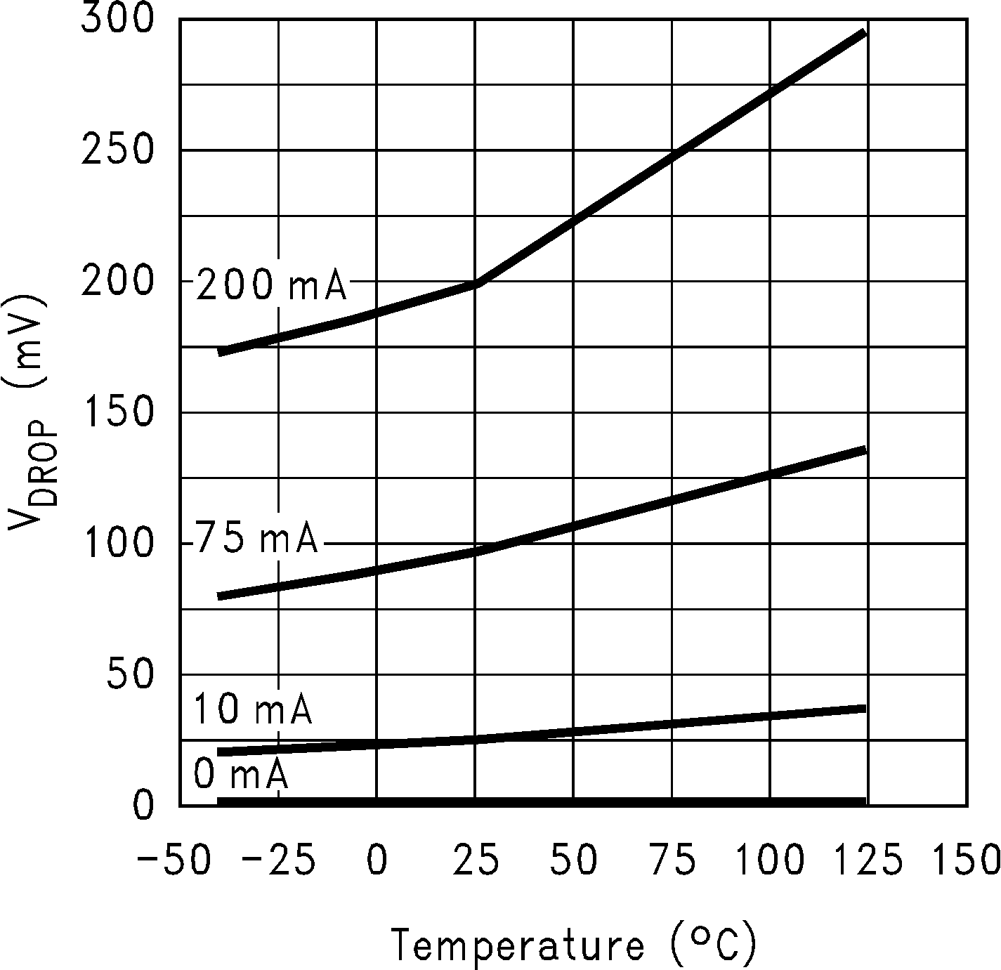
| VIN – VOUT | Dropout voltage(2) | IOUT = 100 µA | 1 | 2 | 1 | 2 | mV | ||
| IOUT = 100 µA –40°C ≤ TJ ≤ 125°C |
3.5 | 3.5 | |||||||
| IOUT = 75 mA | 90 | 120 | 90 | 120 | |||||
| IOUT = 75 mA –40°C ≤ TJ ≤ 125°C |
170 | 170 | |||||||
| IOUT = 200 mA | 180 | 230 | 180 | 230 | |||||
| IOUT = 200 mA –40°C ≤ TJ ≤ 125°C |
350 | 350 | |||||||
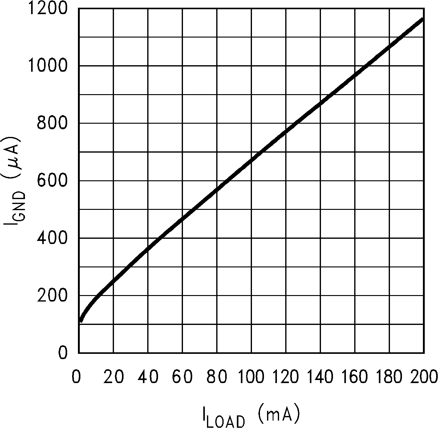
| IGND | Ground pin current | IOUT = 100 µA | 100 | 120 | 100 | 120 | µA | ||
| IOUT = 100 µA –40°C ≤ TJ ≤ 125°C |
150 | 110 | 150 | ||||||
| IOUT = 75 mA | 500 | 800 | 500 | 800 | |||||
| IOUT = 75 mA –40°C ≤ TJ ≤ 125°C |
1400 | 1400 | |||||||
| IOUT = 200 mA | 1 | 2.1 | 1 | 2.1 | mA | ||||
| IOUT = 200 mA –40°C ≤ TJ ≤ 125°C |
3.7 | 3.7 | |||||||
| VSD < 0.3 V | 0.05 | 0.05 | µA | ||||||
| VSD < 0.3 V –40°C ≤ TJ ≤ 125°C |
1.5 | 1.5 | |||||||
| IOUT(PK) | Peak output current | VOUT ≥ VOUT(NOM) − 5% | 250 | 400 | 250 | 400 | mA | ||
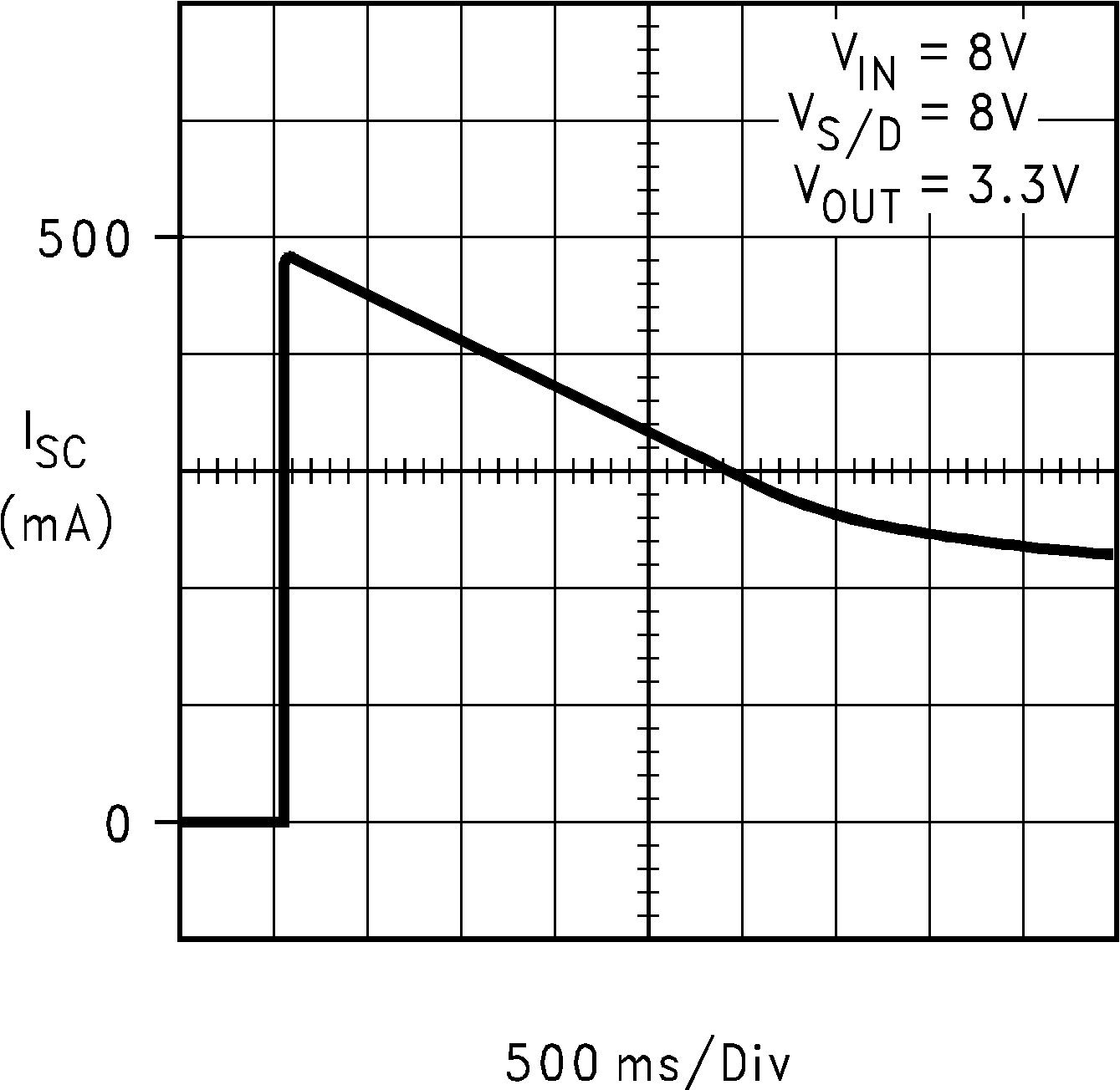
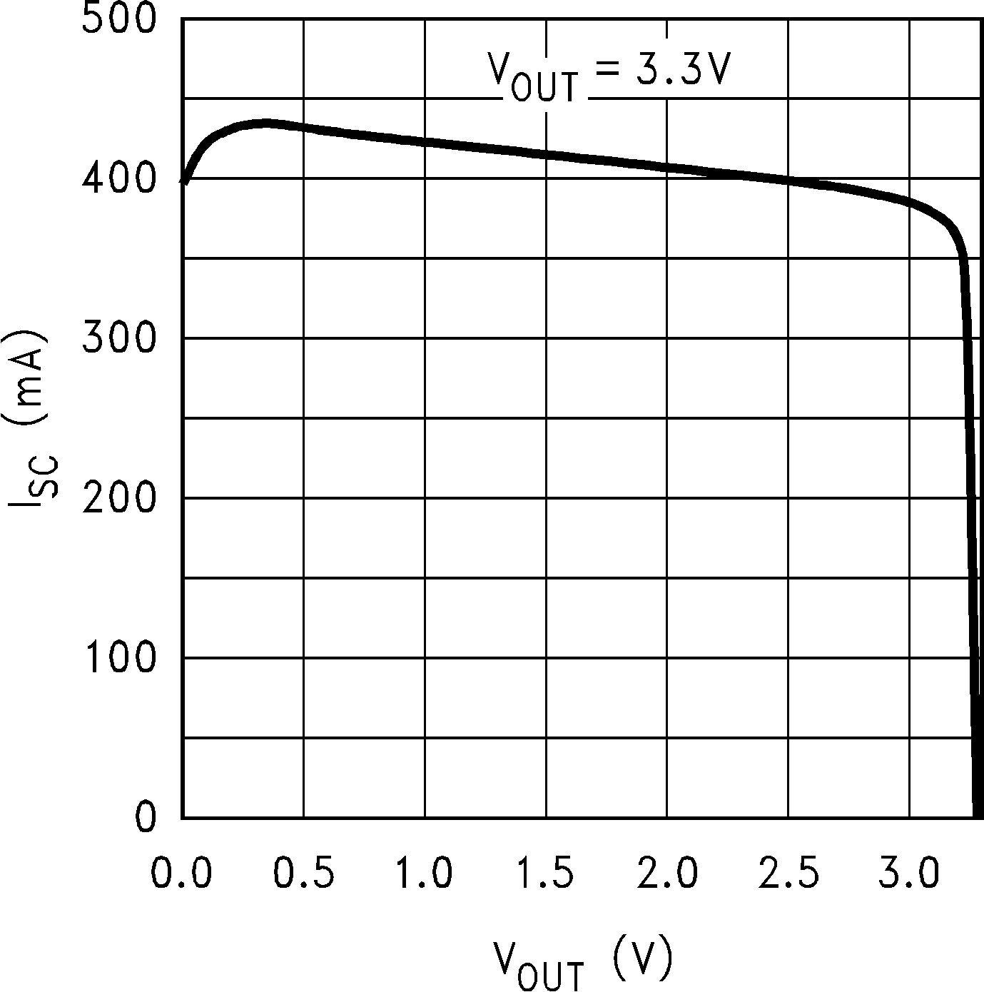
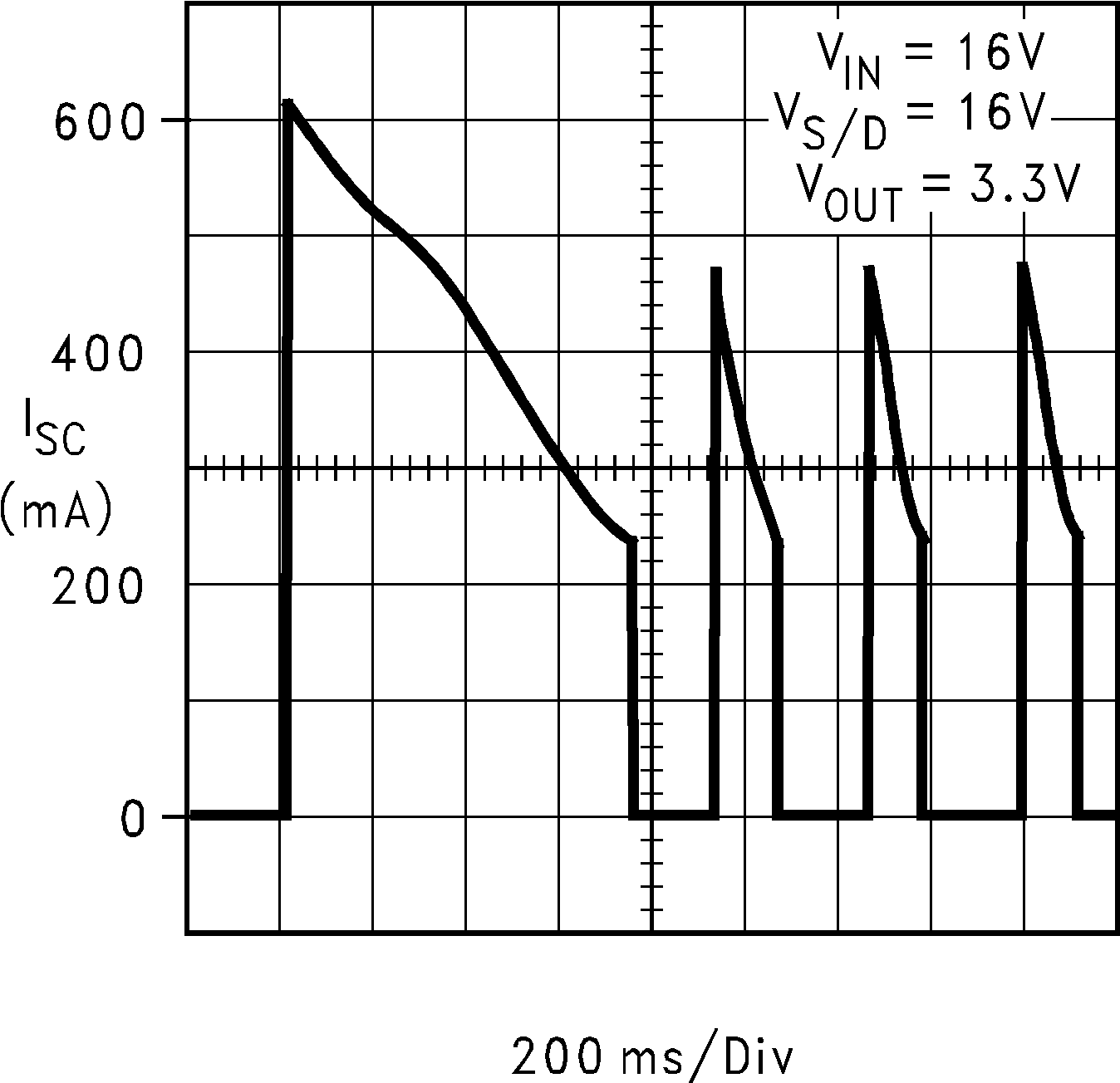
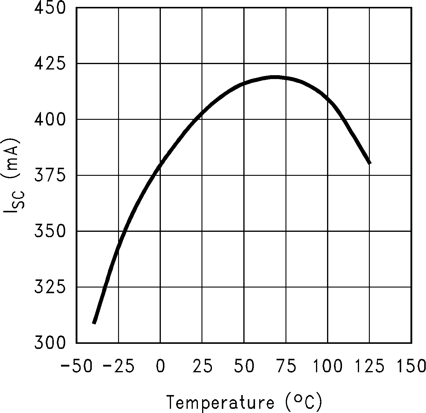
| IOUT(MAX) | Short-circuit current | RL = 0 (steady state)(3) | 400 | 400 | mA | ||||
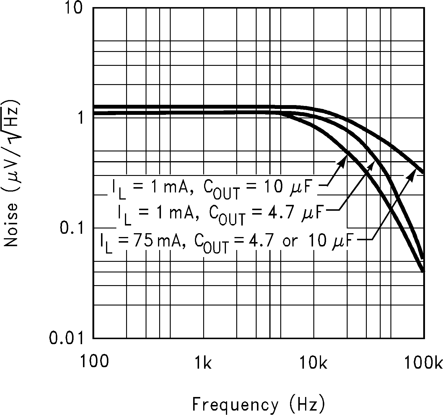
| en | Output noise voltage (RMS) | BW = 300 Hz to 50 kHz, COUT = 10 µF | 160 | 160 | µVRMS | ||||
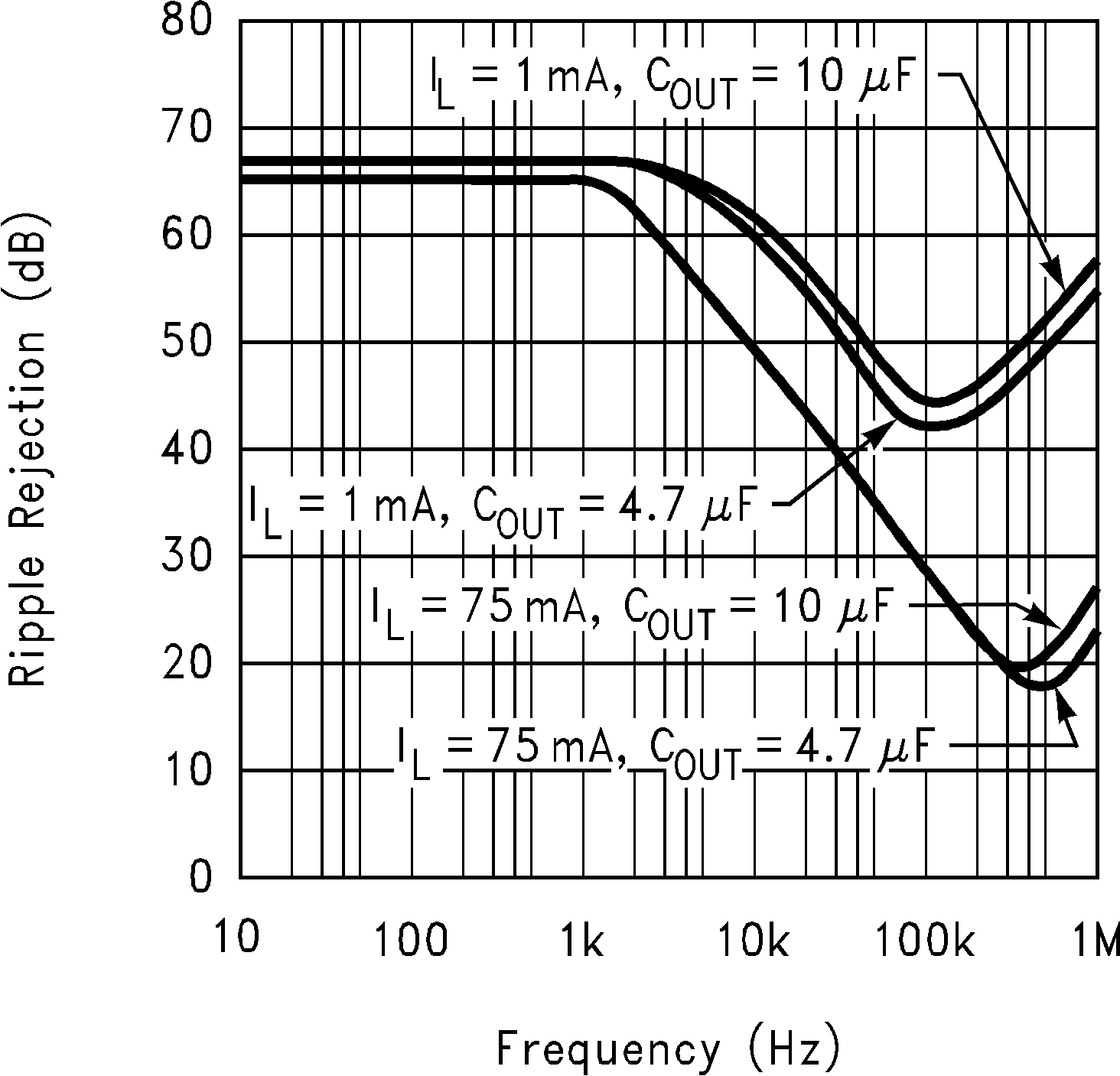
| ΔVOUT/ΔVIN | Ripple rejection | ƒ = 1 kHz, COUT = 10 µF | 65 | 65 | dB | ||||
| ΔVOUT/ΔTD | Output voltage temperature coefficient | See(4) | 20 | 20 | ppm/°C | ||||
| FEEDBACK PIN | |||||||||
| VFB | FEEDBACK pin voltage | 1.21 | 1.23 | 1.25 | 1.2 | 1.23 | 1.26 | V | |
| –40°C ≤ TJ ≤ 125°C | 1.2 | 1.26 | 1.19 | 1.27 | |||||
| See(5) | 1.19 | 1.28 | 1.18 | 1.29 | |||||
| ΔVFB/ΔT | FEEDBACK pin voltage temperature coefficient | See(6) | 20 | 20 | ppm/°C | ||||
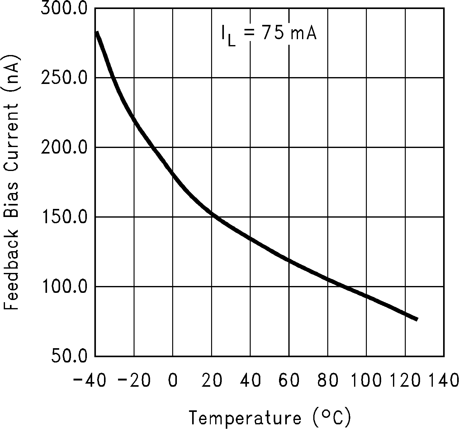
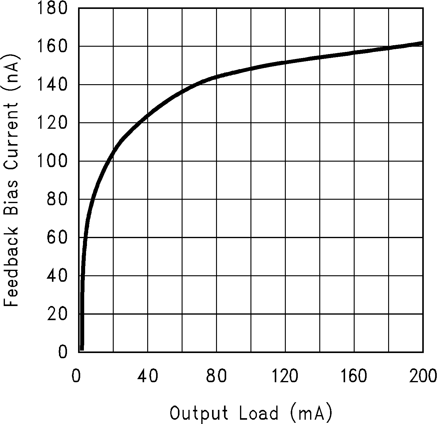
| IFB | FEEDBACK pin bias current | IOUT = 200 mA | 150 | 330 | 150 | 330 | nA | ||
| IOUT = 200 mA –40°C ≤ TJ ≤ 125°C |
760 | 760 | |||||||
| ΔIFB/ΔT | FEEDBACK pin bias current temperature coefficient | See(6) | 0.1 | 0.1 | nA/°C | ||||
| SHUTDOWN INPUT | |||||||||
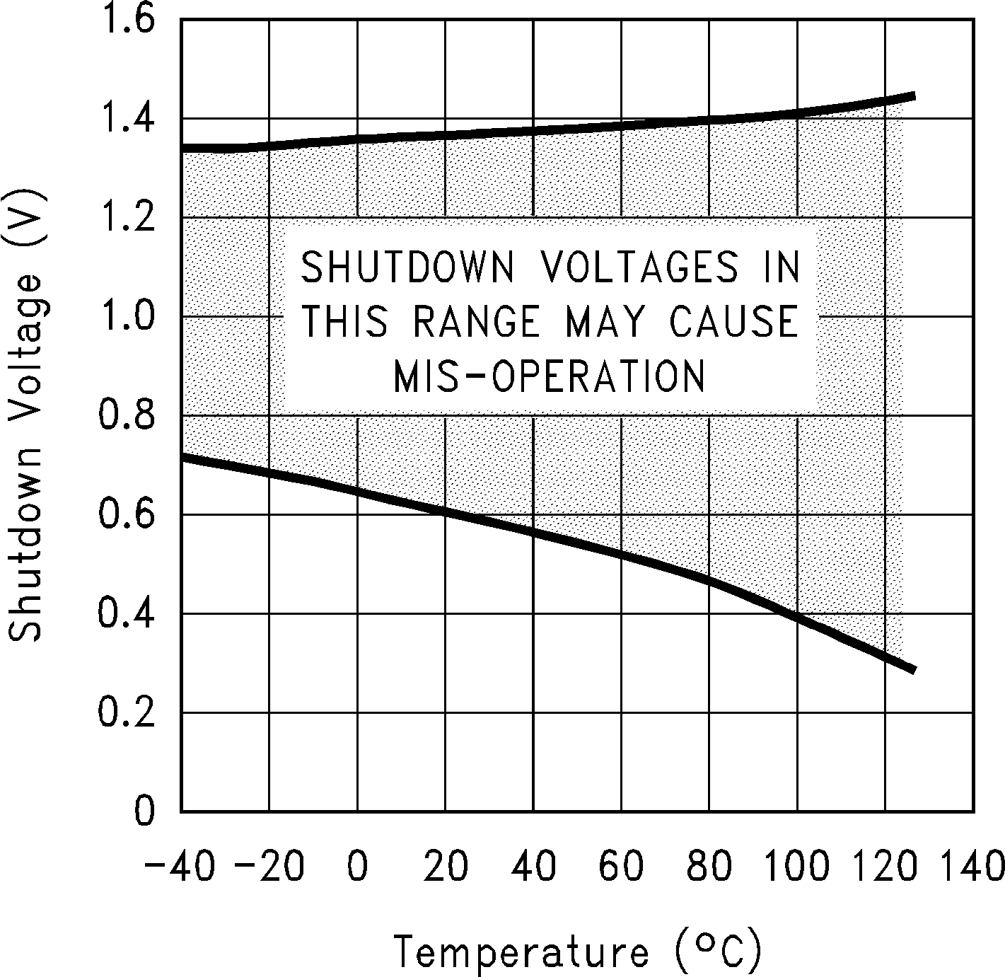
| VSD | SD Input voltage(7) | VH = Output ON | 1.4 | 1.4 | V | ||||
| VH = Output ON –40°C ≤ TJ ≤ 125°C |
1.6 | 1.6 | |||||||
| VL = Output OFF | 0.55 | 0.55 | µA | ||||||
| VL = Output OFF –40°C ≤ TJ ≤ 125°C |
0.18 | 0.18 | |||||||
| ISD | SD Input current | VSD = 0 V | 0 | 0 | V | ||||
| VSD = 0 V, –40°C ≤ TJ ≤ 125°C | –1 | –1 | |||||||
| VSD = 5 V | 5 | 5 | µA | ||||||
| VSD = 5 V, –40°C ≤ TJ ≤ 125°C | 15 | 15 | |||||||
| ERROR COMPARATOR | |||||||||
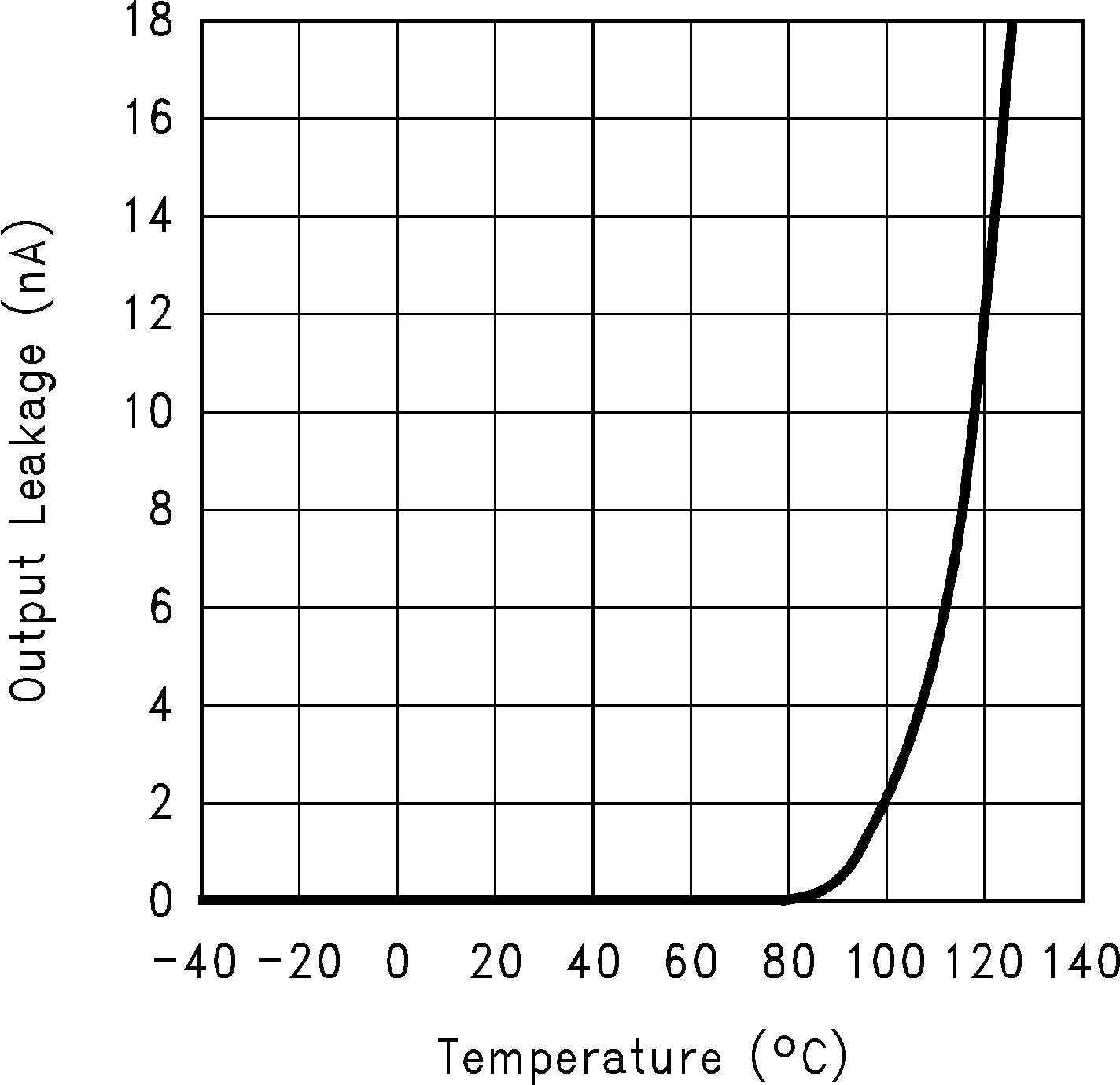
| IOH | Output HIGH leakage | VOH = 16 V | 0.01 | 1 | 0.001 | 1 | µA | ||
| VOH = 16 V, –40°C ≤ TJ ≤ 125°C | 2 | 0.001 | 2 | ||||||
| VOL | Output LOW voltage | VIN = VOUT(NOM) − 0.5 V IOUT(COMP) = 300 µA |
150 | 220 | 150 | 220 | µA | ||
| VIN = VOUT(NOM) − 0.5 V IOUT(COMP) = 300 µA –40°C ≤ TJ ≤ 125°C |
350 | 350 | mV | ||||||
| VTHR(MAX) | Upper threshold voltage | −5.5 | −4.6 | −3.5 | −5.5 | −4.6 | −3.5 | %VOUT | |
| –40°C ≤ TJ ≤ 125°C | −7.7 | −2.5 | −7.7 | −2.5 | |||||
| VTHR(MIN) | Lower threshold voltage | −8.9 | −6.6 | −4.9 | −8.9 | −6.6 | −4.9 | %VOUT | |
| –40°C ≤ TJ ≤ 125°C | −13 | −3.3 | −13 | −3.3 | |||||
| HYST | Hysteresis | 2 | 2 | ||||||
(1) Limits are 100% production tested at 25°C. Limits over the operating temperature range are specified through correlation using Statistical Quality Control (SQC) methods. The limits are used to calculate TI’s Average Outgoing Quality Level (AOQL).
(2) Dropout voltage is defined as the input to output differential at which the output voltage drops 100 mV below the value measured with a 1-V differential.
(3) See the Typical Characteristics section.
(4) Temperature coefficient is defined as the maximum (worst-case) change divided by the total temperature range.
(5) VFB ≤ VOUT ≤ (VIN − 1), 2.5 V ≤ VIN ≤ 16 V, 100 μA ≤ IL ≤ 200 mA, TJ ≤ 125°C.
(6) Temperature coefficient is defined as the maximum (worst-case) change divided by the total temperature range.
(7) To prevent mis-operation, the SHUTDOWN pin must be driven by a signal that swings above VH and below VL with a slew rate not less than 40 mV/μs (see Application and Implementation).
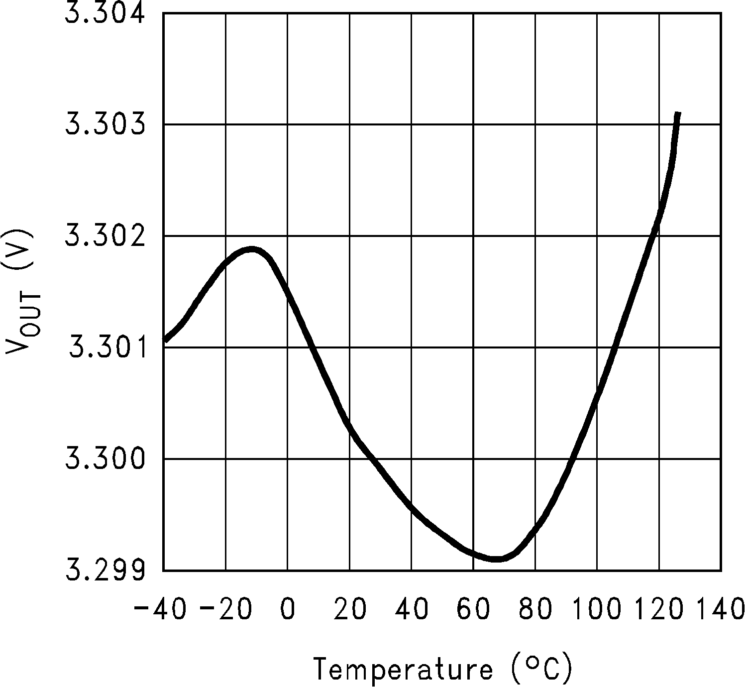
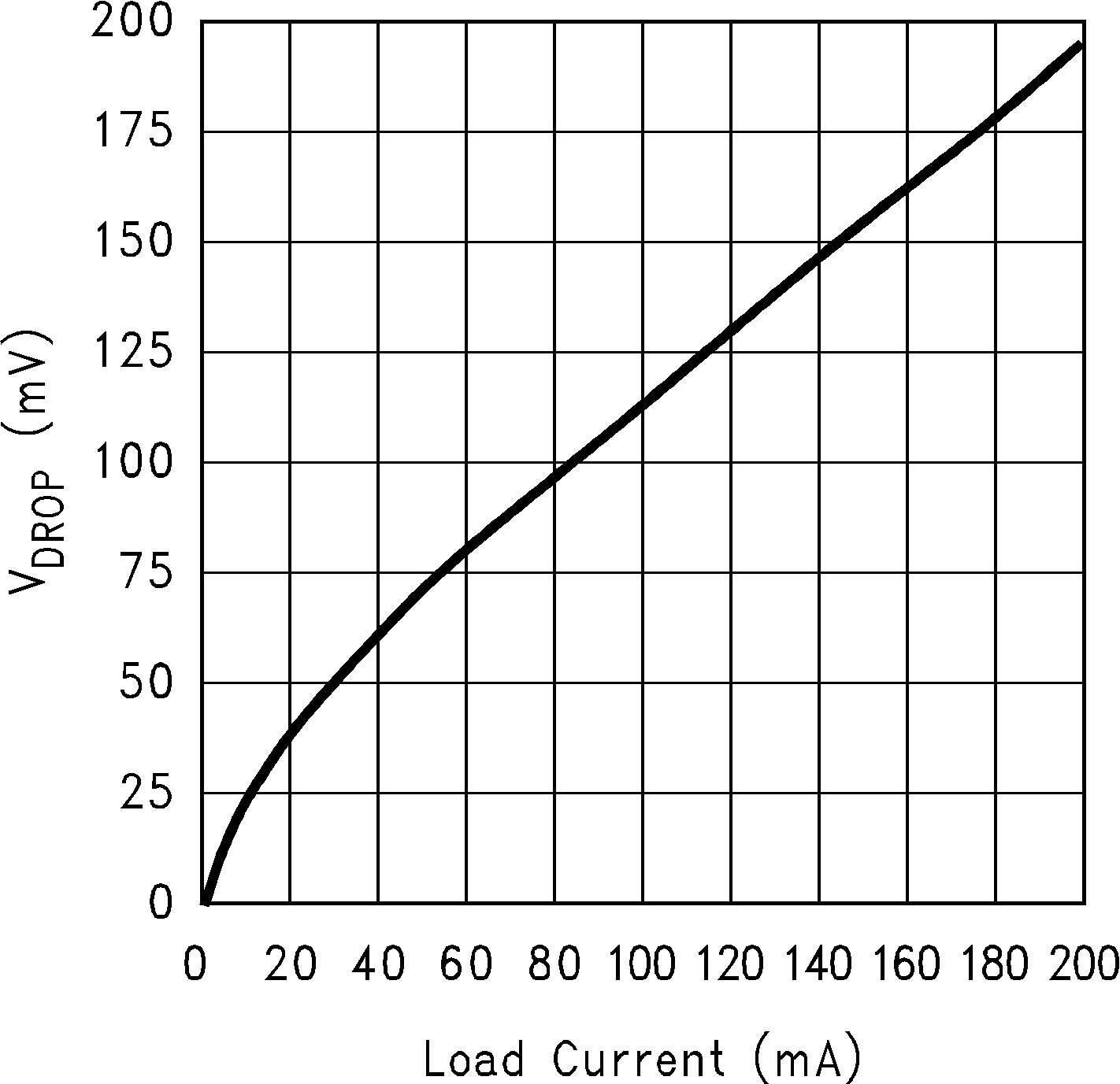
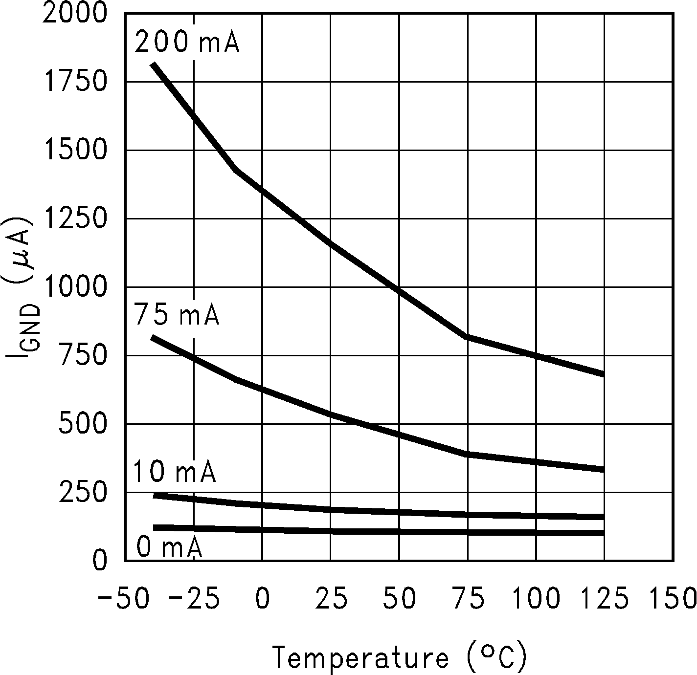
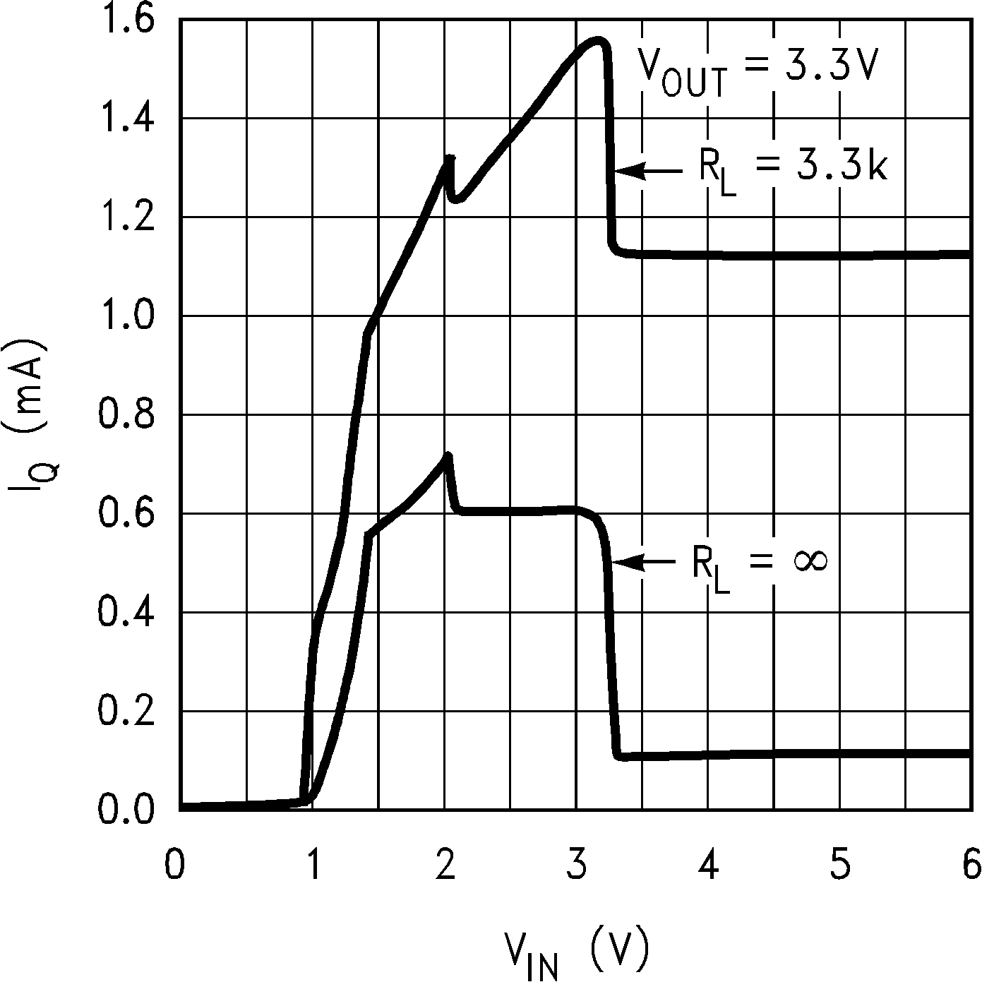
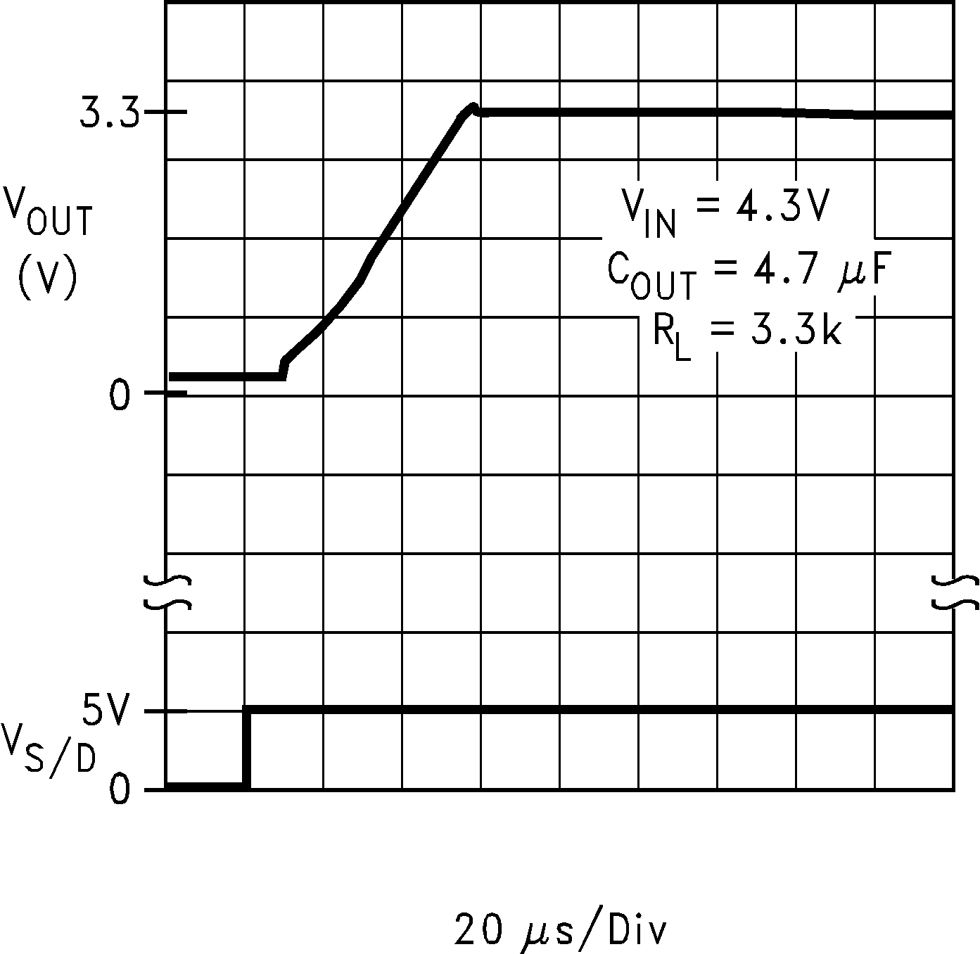
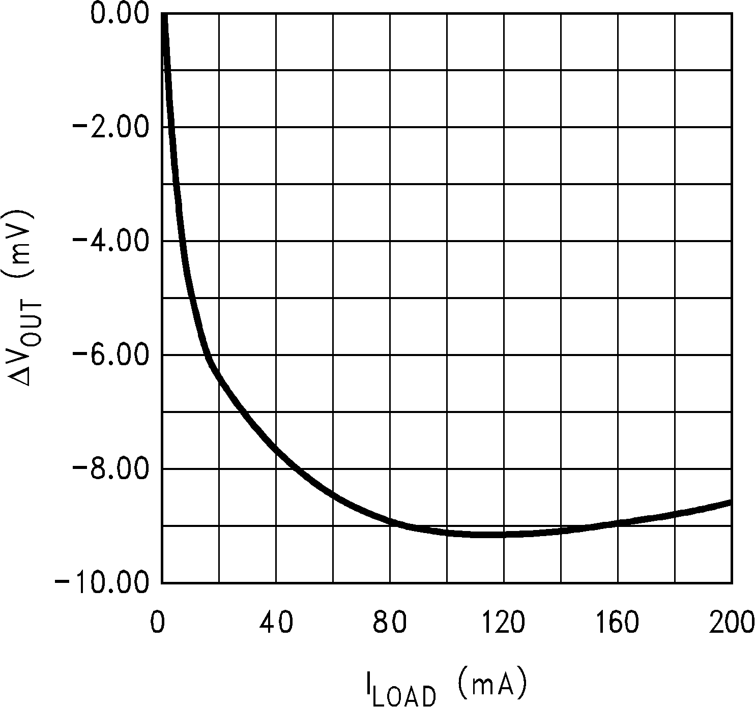
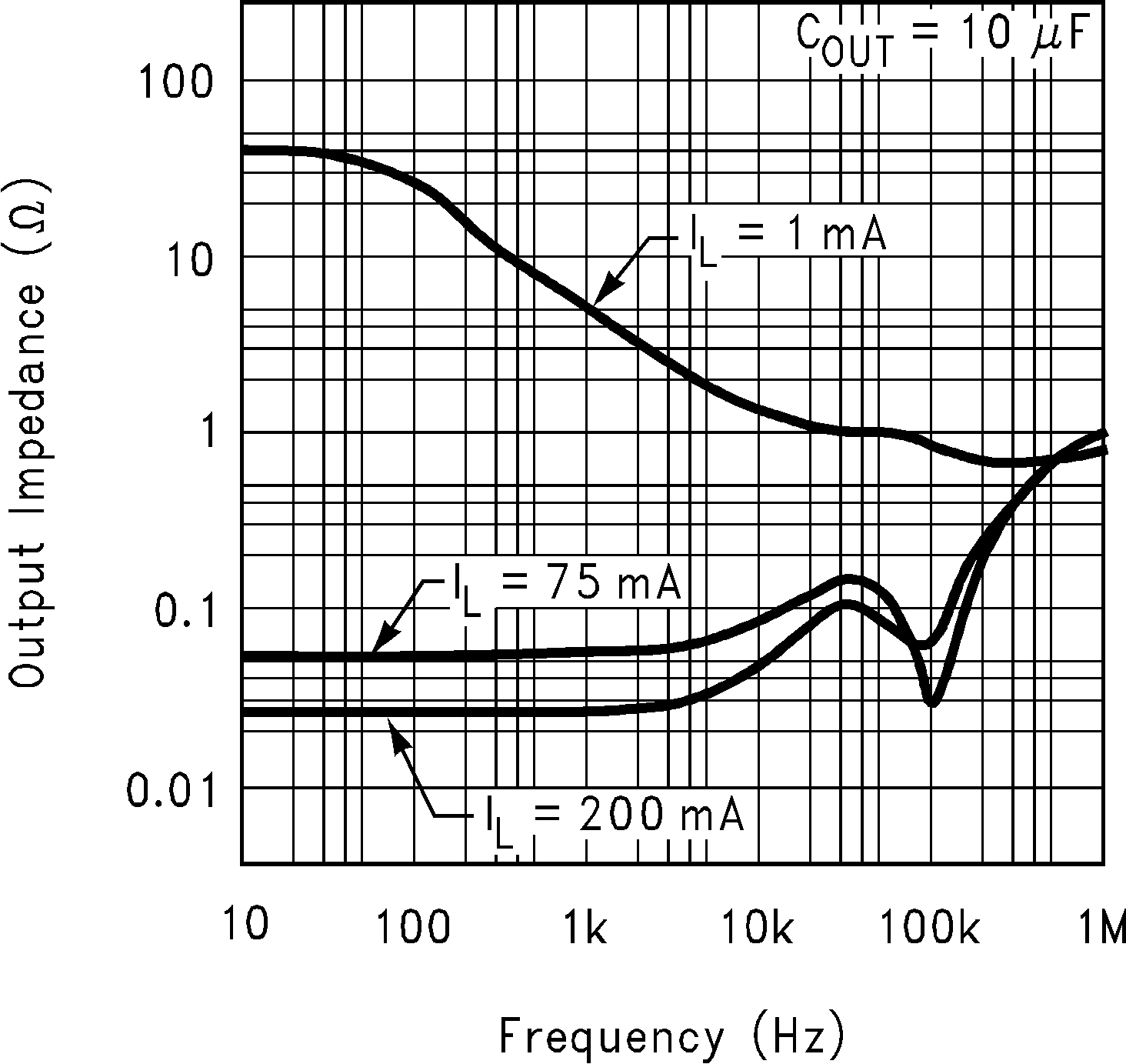
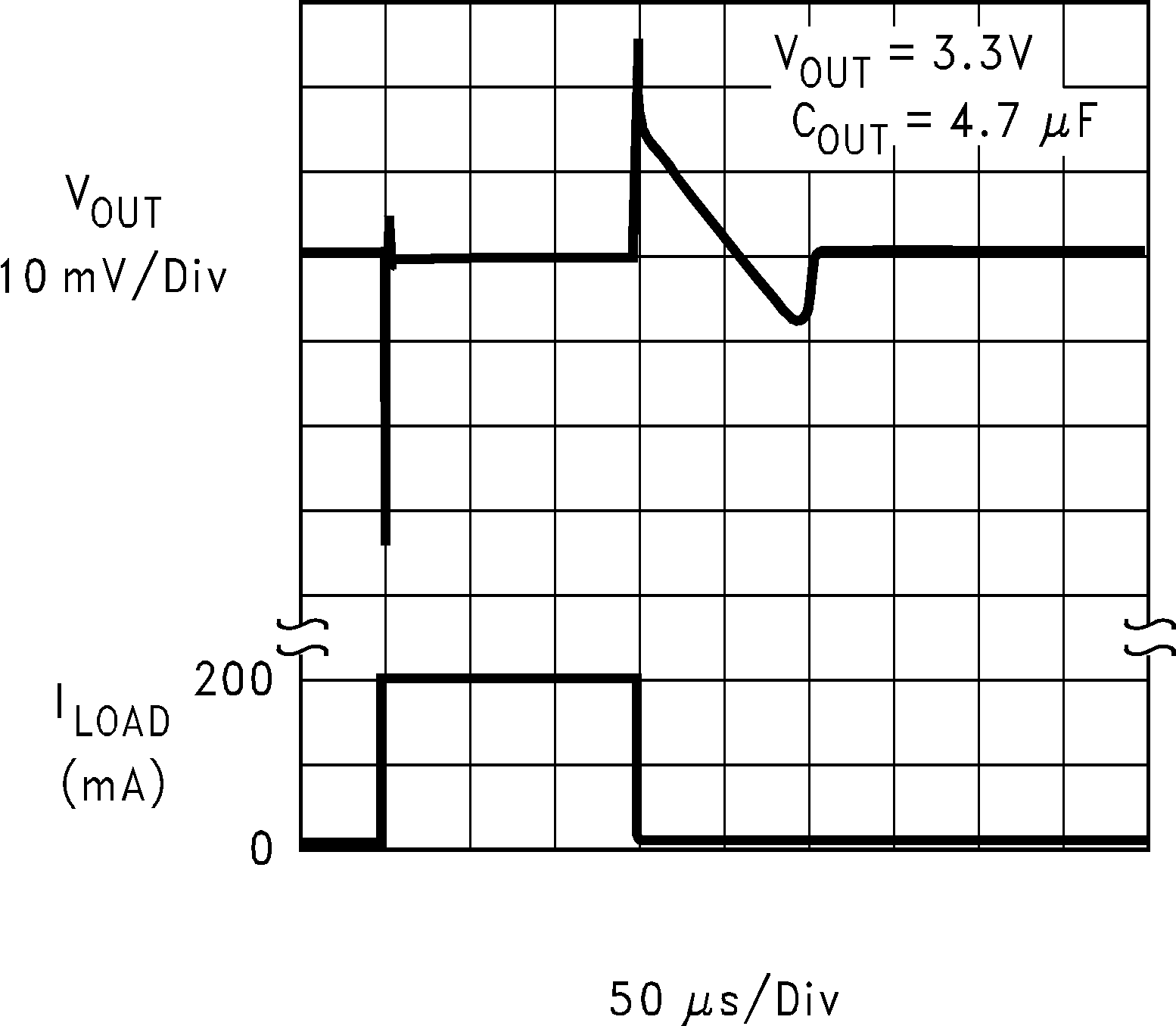
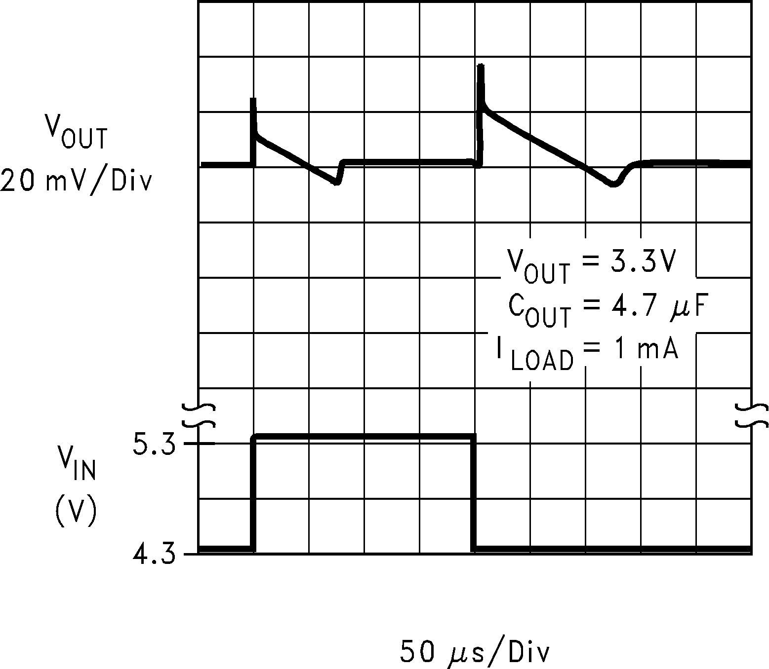
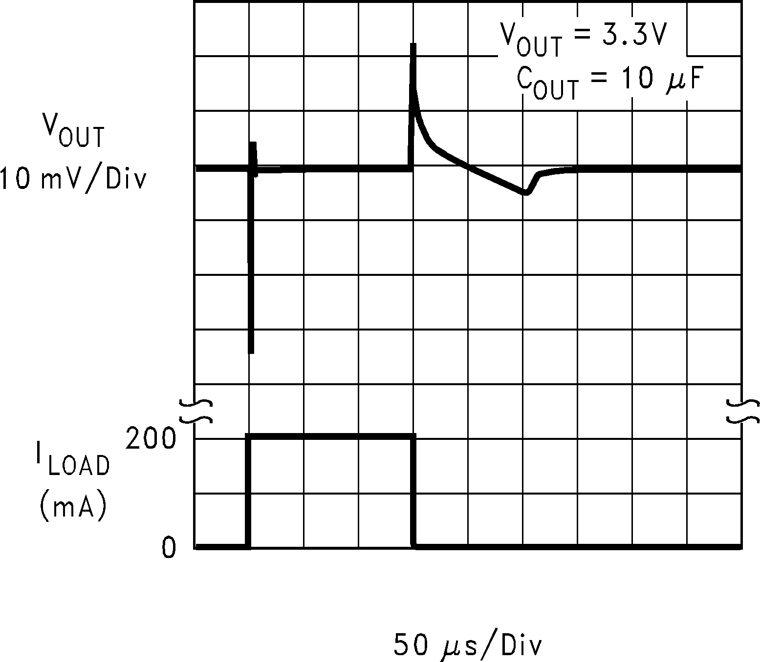
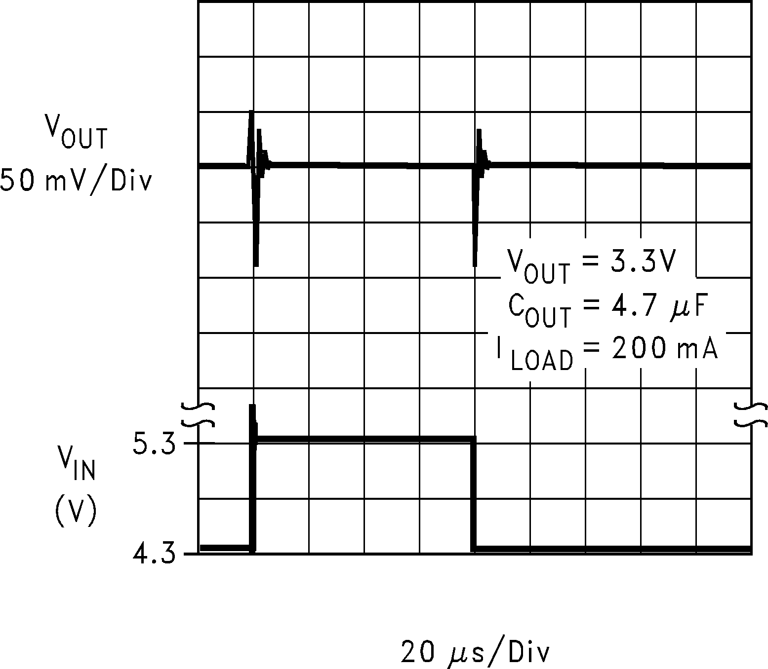
6.6 Typical Characteristics
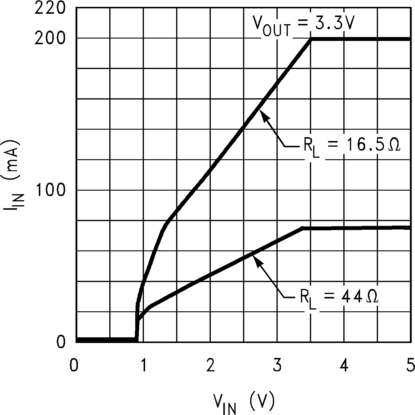
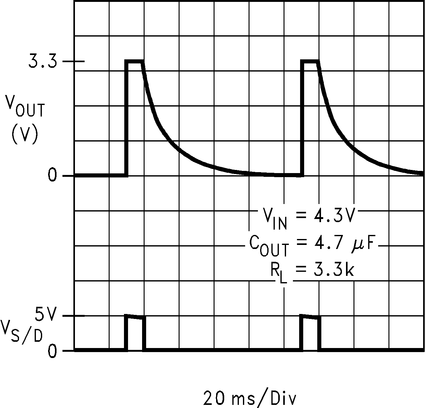
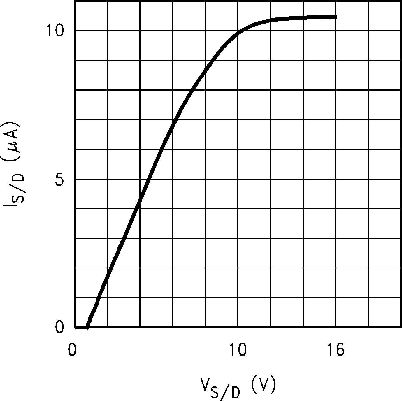
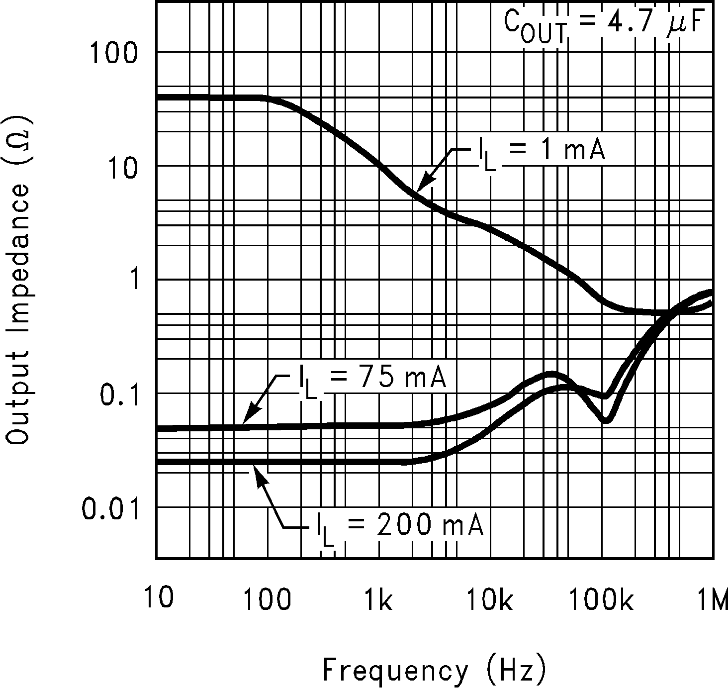
Unless otherwise specified: TA = 25°C, COUT = 4.7 µF, CIN = 2.2 µF, SD is tied to VIN, VIN = VO(NOM) + 1 V, IL = 1 mA.