SNVS361E July 2007 – November 2015 LP38513
PRODUCTION DATA.
- 1 Features
- 2 Applications
- 3 Description
- 4 Revision History
- 5 Pin Configuration and Functions
- 6 Specifications
- 7 Detailed Description
- 8 Application and Implementation
- 9 Power Supply Recommendations
- 10Layout
- 11Device and Documentation Support
- 12Mechanical, Packaging, and Orderable Information
封装选项
机械数据 (封装 | 引脚)
散热焊盘机械数据 (封装 | 引脚)
- KTT|5
订购信息
10 Layout
10.1 Layout Guidelines
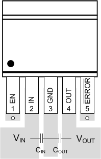
The dynamic performance of the LP38513 is dependent on the layout of the PCB. PCB layout practices that are adequate for typical LDOs may degrade the PSRR, noise, or transient performance of the device. Best performance is achieved by placing CIN and COUT on the same side of the PCB as the LP38513, and as close to the package as is practical. The ground connections for CIN and COUT must be back to the LP38513 GND pin using as wide and short of a copper trace as is practical.
Good PC layout practices must be used or instability can be induced because of ground loops and voltage drops. The input and output capacitors must be directly connected to the IN, OUT, and GND pins of the LP38513 using traces which do not have other currents flowing in them (Kelvin connect). The best way to do this is to lay out CIN and COUT near the device with short traces to the IN, OUT, and GND pins. The regulator ground pin must be connected to the external circuit ground so that the regulator and its capacitors have a single-point ground.
Stability problems have been seen in applications where vias to an internal ground plane were used at the ground points of the LP38513 device and the input and output capacitors. This was caused by varying ground potentials at these nodes resulting from current flowing through the ground plane. Using a single point ground technique for the regulator and its capacitors fixed the problem.
Because high current flows through the traces going into the IN pin and coming from the OUT pin, Kelvin connect the capacitor leads to these pins so there is no voltage drop in series with the input and output capacitors.
10.2 Layout Example
 Figure 24. LP38513 Layout