ZHCSAZ8K January 2005 – January 2016 LP38691-ADJ , LP38691-ADJ-Q1 , LP38693-ADJ , LP38693-ADJ-Q1
PRODUCTION DATA.
- 1 特性
- 2 应用范围
- 3 说明
- 4 修订历史记录
- 5 Pin Configuration and Functions
- 6 Specifications
- 7 Detailed Description
-
8 Application and Implementation
- 8.1 Application Information
- 8.2
Typical Applications
- 8.2.1 Design Requirements
- 8.2.2 Detailed Design Procedure
- 8.2.3 Application Curve
- 9 Power Supply Recommendations
- 10Layout
- 11器件和文档支持
- 12机械、封装和可订购信息
8 Application and Implementation
NOTE
Information in the following applications sections is not part of the TI component specification, and TI does not warrant its accuracy or completeness. TI’s customers are responsible for determining suitability of components for their purposes. Customers should validate and test their design implementation to confirm system functionality.
8.1 Application Information
The LP3869x-ADJ can provide 500 mA output current with 2.7 V to 10 V input. Adjustable output voltage in the range of 1.25 V to 9 V. LP3869x-ADJ is stable with a 1-μF ceramic output capacitor. Typical output noise is
0.7 μVRMS at frequencies from 10 Hz to 10 kHz. Typical PSSR is 55 dB at 1 kHz.
8.2 Typical Applications


8.2.1 Design Requirements
For typical LDO CMOS linear regulators , use the parameters listed in Table 1.
Table 1. Design Parameters
| DESIGN PARAMETERS | EXAMPLE VALUE |
|---|---|
| Input voltage range | 2.7 V to 10 V |
| Output range | Adjustable |
| Output current | 500 mA (maximum) |
| Output capacitor range | 1 µF |
8.2.2 Detailed Design Procedure
8.2.2.1 Setting the Output Voltage
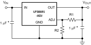
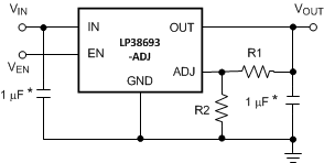
The output voltage is set using the external resistors R1 and R2 (see Typical Applications. The output voltage will be given by Equation 1:
Because the part has a minimum load current requirement of 100 μA, it is recommended that R2 always be 12 kΩ or less to provide adequate loading. Even if a minimum load is always provided by other means, it is not recommended that very high value resistors be used for R1 and R2 because it can make the ADJ node susceptible to noise pickup. A maximum Ohmic value of 100 kΩ is recommended for R2 to prevent this from occurring.
8.2.2.2 External Capacitors
In common with most regulators, the LP3869x-ADJ devices require an external capacitors for regulator stability. The devices are specifically designed for portable applications requiring minimum board space and smallest components. These capacitors must be correctly selected for good performance.
8.2.2.3 Input Capacitor
An input capacitor of at least 1 μF is required (ceramic recommended). The capacitor must be located not more than one centimeter from the input pin and returned to a clean analog ground.
8.2.2.4 Output Capacitor
An output capacitor is required for loop stability. It must be located less than 1 centimeter from the device and connected directly to the output and ground pins using traces which have no other currents flowing through them.
The minimum amount of output capacitance that can be used for stable operation is 1 μF. Ceramic capacitors are recommended; the LP3869x-ADJ devices were designed for use with ultra-low equivalent series resistance (ESR) capacitors. The LP3869x-ADJ is stable with any output capacitor ESR between 5 mΩ to 500 mΩ.
8.2.2.5 Capacitor Characteristics
It is important that capacitance tolerance and variation with temperature be taken into consideration when selecting a capacitor so that the minimum required amount of capacitance is provided over the full operating temperature range.
8.2.2.5.1 Ceramic Capacitors
For values of capacitance in the 10- to 100-μF range, ceramics are usually larger and more costly than tantalums but give superior AC performance for bypassing high frequency noise because of very low ESR (typically less than 10 mΩ). However, some dielectric types do not have good capacitance characteristics as a function of voltage and temperature.
The LP3869x-ADJ is designed to work with ceramic capacitors on the output to take advantage of the benefits they offer. For capacitance values in the range of 0.47 µF to 4.7 µF, ceramic capacitors are the smallest, least expensive and have the lowest ESR values, thus making them best for eliminating high frequency noise. The ESR of a typical 1-µF ceramic capacitor is in the range of 20 mΩ to 40 mΩ, which easily meets the ESR requirement for stability for the LP3869x.
Z5U and Y5V dielectric ceramics have capacitance that drops severely with applied voltage. A typical Z5U or Y5V capacitor can lose 60% of its rated capacitance with half of the rated voltage applied to it. The Z5U and Y5V also exhibit a severe temperature effect, losing more than 50% of nominal capacitance at high and low limits of the temperature range.
X7R and X5R dielectric ceramic capacitors are strongly recommended if ceramics are used, as they typically maintain a capacitance range within ±20% of nominal over full operating ratings of temperature and voltage. Of course, they are typically larger and more costly than Z5U/Y5U types for a given voltage and capacitance.
8.2.2.5.2 Tantalum Capacitors
Solid tantalum capacitors have good temperature stability: a high-quality tantalum capacitor typically shows a capacitance value that varies less than 10-15% across the full temperature range of -40°C to 125°C. ESR will vary only about 2× going from the high to low temperature limits.
The increasing ESR at lower temperatures can cause oscillations when marginal quality capacitors are used (if the ESR of the capacitor is near the upper limit of the stability range at room temperature).
8.2.2.6 RFI/EMI Susceptibility
Radio frequency interference (RFI) and electromagnetic interference (EMI) can degrade the performance of any integrated circuit because of the small dimensions of the geometries inside the device. In applications where circuit sources are present which generate signals with significant high frequency energy content (> 1 MHz), care must be taken to ensure that this does not affect the device regulator.
If RFI/EMI noise is present on the input side of the regulator (such as applications where the input source comes from the output of a switching regulator), good ceramic bypass capacitors must be used at the input pin of the device.
If a load is connected to the device output which switches at high speed (such as a clock), the high-frequency current pulses required by the load must be supplied by the capacitors on the device output. Because the bandwidth of the regulator loop is less than 100 kHz, the control circuitry cannot respond to load changes above that frequency. This means the effective output impedance of the device at frequencies above 100 kHz is determined only by the output capacitors.
In applications where the load is switching at high speed, the output of the device may need RF isolation from the load. It is recommended that some inductance be placed between the output capacitor and the load, and good RF bypass capacitors be placed directly across the load.
PCB layout is also critical in high noise environments, because RFI/EMI is easily radiated directly into PC traces. Noisy circuitry should be isolated from clean circuits where possible, and grounded through a separate path. At MHz frequencies, ground planes begin to look inductive and RFI/ EMI can cause ground bounce across the ground plane. In multi-layer PCB applications, care should be taken in layout so that noisy power and ground planes do not radiate directly into adjacent layers which carry analog power and ground.
8.2.2.7 Output Noise
Noise is specified in two ways:
- Spot Noise or Output Noise Density is the RMS sum of all noise sources, measured at the regulator output, at a specific frequency (measured with a 1-Hz bandwidth). This type of noise is usually plotted on a curve as a function of frequency.
- Total Output Noise or Broad-Band Noise is the RMS sum of spot noise over a specified bandwidth, usually several decades of frequencies.
Attention should be paid to the units of measurement. Spot noise is measured in units µV√Hz or nV√Hz, and total output noise is measured in µVRMS.
The primary source of noise in low-dropout regulators is the internal reference. Noise can be reduced in two ways: by increasing the transistor area or by increasing the current drawn by the internal reference. Increasing the area will decrease the chance of fitting the die into a smaller package. Increasing the current drawn by the internal reference increases the total supply current (GND pin current).
8.2.2.8 Power Dissipation
Knowing the device power dissipation and proper sizing of the thermal plane connected to the tab or pad is critical to ensuring reliable operation. Device power dissipation depends on input voltage, output voltage, and load conditions and can be calculated with Equation 2.
Power dissipation can be minimized, and greater efficiency can be achieved, by using the lowest available voltage drop option that would still be greater than the dropout voltage (VDO). However, keep in mind that higher voltage drops result in better dynamic (that is, PSRR and transient) performance.
On the WSON (DRV) package, the primary conduction path for heat is through the exposed power pad to the PCB. To ensure the device does not overheat, connect the exposed pad, through thermal vias, to an internal ground plane with an appropriate amount of copper PCB area .
On the VSSOP (DGK) and SOT-223 (NDC) packages, the primary conduction path for heat is through the pins to the PCB.
The maximum allowable junction temperature (TJ(MAX)) determines maximum power dissipation allowed (PD(MAX)) for the device package.
Power dissipation and junction temperature are most often related by the junction-to-ambient thermal resistance (RθJA) of the combined PCB and device package and the temperature of the ambient air (TA), according to Equation 3 or Equation 4:
Unfortunately, this RθJA is highly dependent on the heat-spreading capability of the particular PCB design, and therefore varies according to the total copper area, copper weight, and location of the planes. The RθJA recorded in Thermal Information is determined by the specific EIA/JEDEC JESD51-7 standard for PCB and copper-spreading area, and is to be used only as a relative measure of package thermal performance. For a well-designed thermal layout, RθJA is actually the sum of the package junction-to-case (bottom) thermal resistance (RθJCbot) plus the thermal resistance contribution by the PCB copper area acting as a heat sink.
8.2.2.9 Estimating Junction Temperature
The EIA/JEDEC standard recommends the use of psi (Ψ) thermal characteristics to estimate the junction temperatures of surface mount devices on a typical PCB board application. These characteristics are not true thermal resistance values, but rather package specific thermal characteristics that offer practical and relative means of estimating junction temperatures. These psi metrics are determined to be significantly independent of copper-spreading area. The key thermal characteristics (ΨJT and ΨJB) are given in Thermal Information and are used in accordance with Equation 5 or Equation 6.
where
- PD(MAX) is explained in Equation 2.
- TTOP is the temperature measured at the center-top of the device package.
where
- PD(MAX) is explained in Equation 2.
- TBOARD is the PCB surface temperature measured 1-mm from the device package and centered on the package edge.
For more information about the thermal characteristics ΨJT and ΨJB, see the TI Application Report Semiconductor and IC Package Thermal Metrics (SPRA953), available for download at www.ti.com.
For more information about measuring TTOP and TBOARD, see the TI Application Report Using New Thermal Metrics (SBVA025), available for download at www.ti.com.
For more information about the EIA/JEDEC JESD51 PCB used for validating RθJA, see the TI Application Report Thermal Characteristics of Linear and Logic Packages Using JEDEC PCB Designs (SZZA017), available for download at www.ti.com.
8.2.2.10 Reverse Voltage
A reverse voltage condition will exist when the voltage at the OUT pin is higher than the voltage at the IN pin. Typically this will happen when VIN is abruptly taken low and COUT continues to hold a sufficient charge such that the input to output voltage becomes reversed. A less common condition is when an alternate voltage source is connected to the output.
There are two possible paths for current to flow from the OUT pin back to IN during a reverse voltage condition.
- While VIN is high enough to keep the control circuity alive, and the EN pin (LP38693-ADJ only) is above the VEN(ON) threshold, the control circuitry will attempt to regulate the output voltage. If the input voltage is less than the programmed output voltage, the control circuit will drive the gate of the pass element to the full ON condition. In this condition, reverse current will flow from the OUT to the IN pin, limited only by the RDS(ON) of the pass element and the output to input voltage differential. Discharging an output capacitor up to 1000 μF in this manner will not damage the device as the current will rapidly decay. However, continuous reverse current should be avoided. When the EN pin is low, this condition will be prevented.
- The internal PFET pass element has an inherent parasitic diode. During normal operation, the input voltage is higher than the output voltage and the parasitic diode is reverse biased. However, when VIN is below the value where the control circuity is alive, or the EN pin is low (LP38693-ADJ only), and the output voltage is more than 500 mV (typical) above the input voltage the parasitic diode becomes forward biased and current flows from the output pin to the input pin through the diode. The current in the parasitic diode should be limited to less than 1-A continuous and 5-A peak.
If used in a dual-supply system where the regulator output load is returned to a negative supply, the OUT pin must be diode clamped to ground to limit the negative voltage transition. A Schottky diode is recommended for this protective clamp.
8.2.3 Application Curve
