ZHCSAS0L January 2005 – December 2014 LP38691 , LP38691-Q1 , LP38693 , LP38693-Q1
PRODUCTION DATA.
- 1 特性
- 2 应用范围
- 3 说明
- 4 典型应用电路
- 5 修订历史记录
- 6 Pin Configuration and Functions
- 7 Specifications
- 8 Detailed Description
- 9 Application and Implementation
- 10Power Supply Recommendations
- 11Layout
- 12器件和文档支持
- 13机械封装和可订购信息
9 Application and Implementation
NOTE
Information in the following applications sections is not part of the TI component specification, and TI does not warrant its accuracy or completeness. TI’s customers are responsible for determining suitability of components for their purposes. Customers should validate and test their design implementation to confirm system functionality.
9.1 Application Information
9.1.1 Reverse Voltage
A reverse voltage condition will exist when the voltage at the output pin is higher than the voltage at the input pin. Typically this will happen when VIN is abruptly taken low and COUT continues to hold a sufficient charge such that the input to output voltage becomes reversed. A less common condition is when an alternate voltage source is connected to the output.
There are two possible paths for current to flow from the output pin back to the input during a reverse voltage condition.
- While VIN is high enough to keep the control circuity alive, and the Enable pin (LP38693 only) is above the VEN(ON) threshold, the control circuitry will attempt to regulate the output voltage. If the input voltage is less than the programmed output voltage, the control circuit will drive the gate of the pass element to the full ON condition. In this condition, reverse current will flow from the output pin to the input pin, limited only by the RDS(ON) of the pass element and the output to input voltage differential. Discharging an output capacitor up to 1000 μF in this manner will not damage the device as the current will rapidly decay. However, continuous reverse current should be avoided. When the Enable pin is low this condition will be prevented.
- The internal PFET pass element has an inherent parasitic diode. During normal operation, the input voltage is higher than the output voltage and the parasitic diode is reverse biased. However, when VIN is below the value where the control circuity is alive, or the Enable pin is low (LP38693 only), and the output voltage is more than 500 mV (typical) above the input voltage the parasitic diode becomes forward biased and current flows from the output pin to the input pin through the diode. The current in the parasitic diode should be limited to less than 1A continuous and 5A peak.
If used in a dual-supply system where the regulator output load is returned to a negative supply, the output pin must be diode clamped to ground to limit the negative voltage transition. A Schottky diode is recommended for this protective clamp.
9.2 Typical Application
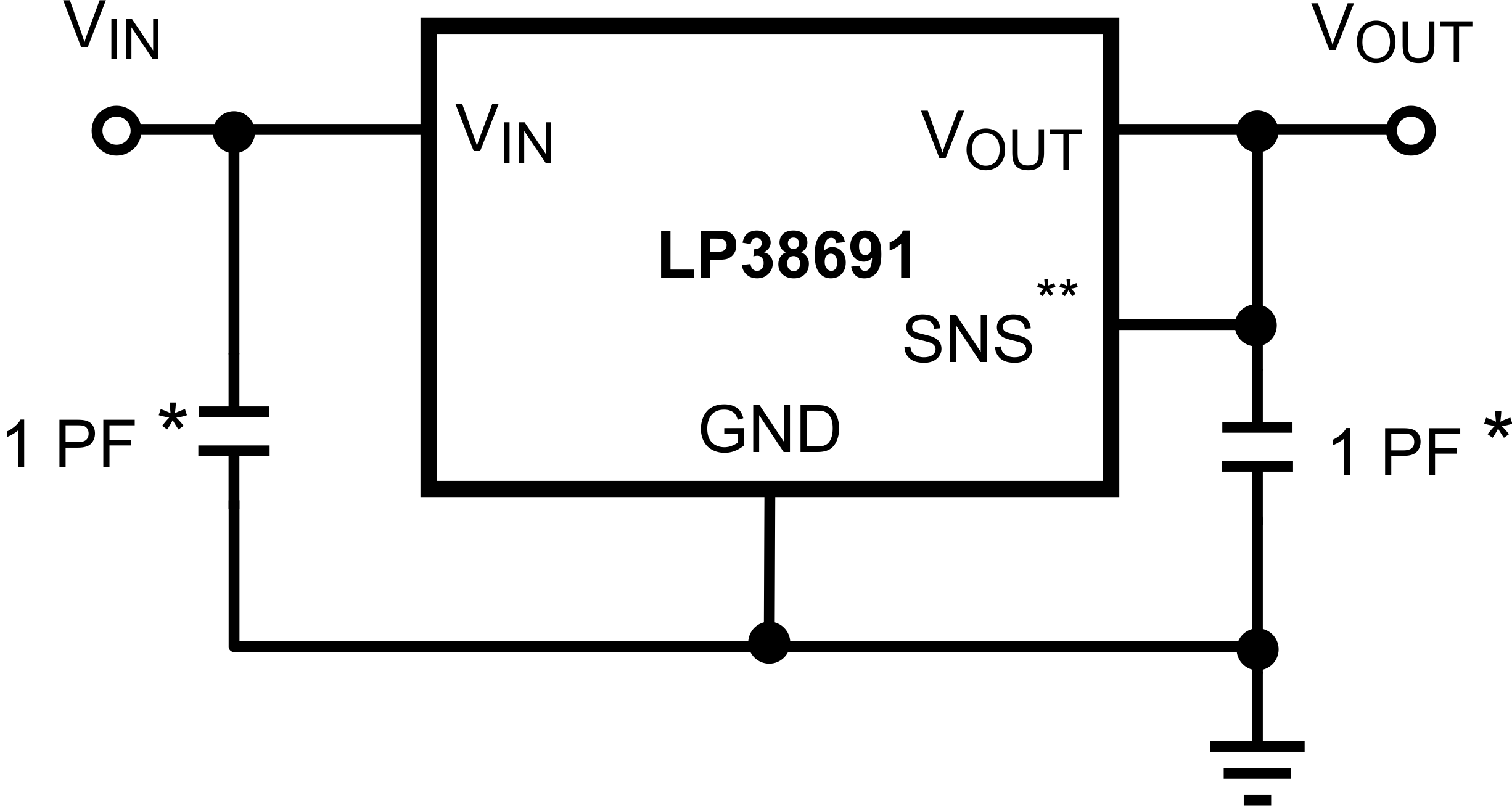
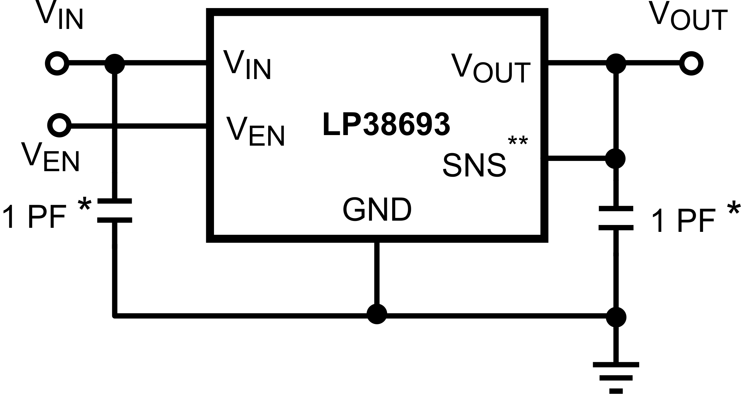
**WSON package devices only.
9.2.1 Design Requirements
Table 1. Design Parameters
| DESIGN PARAMETERS | EXAMPLE VALUE |
|---|---|
| Input voltage range | 2.7 V to 10 V |
| Output range | 1.8 V |
| Output current | 1 A |
| Output capacitor range | 1 µF |
| Input and output capacitor ESR range | 5 mΩ to 500 mΩ |
9.2.2 Detailed Design Procedure
To begin the design process, determine the following:
- Available input voltage range
- Output voltage needed
- Output current needed
- Input and output capacitors
9.2.2.1 Power Dissipation and Device Operation
The permissible power dissipation for any package is a measure of the capability of the device to pass heat from the power source, the junctions of the IC, to the ultimate heat sink, the ambient environment. Thus, the power dissipation is dependent on the ambient temperature and the thermal resistance across the various interfaces between the die junction and ambient air.
The maximum allowable power dissipation for the device in a given package can be calculated using Equation 1:
The actual power being dissipated in the device can be represented by Equation 2:
These two equations establish the relationship between the maximum power dissipation allowed due to thermal consideration, the voltage drop across the device, and the continuous current capability of the device. These two equations should be used to determine the optimum operating conditions for the device in the application.
In applications where lower power dissipation (PD) and/or excellent package thermal resistance (RθJA) is present, the maximum ambient temperature (TA-MAX) may be increased.
In applications where high power dissipation and/or poor package thermal resistance is present, the maximum ambient temperature (TA-MAX) may have to be derated. TA-MAX is dependent on the maximum operating junction temperature (TJ-MAX-OP = 125°C), the maximum allowable power dissipation in the device package in the application (PD-MAX), and the junction-to ambient thermal resistance of the part/package in the application (RθJA), as given by Equation 3:
Alternately, if TA-MAX can not be derated, the PD value must be reduced. This can be accomplished by reducing VIN in the 'VIN–VOUT' term as long as the minimum VIN is met, or by reducing the IOUT term, or by some combination of the two.
9.2.2.2 External Capacitors
In common with most regulators, the LP3869x requires external capacitors for regulator stability. The LP3869x is specifically designed for portable applications requiring minimum board space and smallest components. These capacitors must be correctly selected for good performance.
9.2.2.3 Input Capacitor
An input capacitor is required for stability. It is recommended that a 1-µF capacitor be connected between the LP3869x IN pin and GND pin (this capacitance value may be increased without limit).
This capacitor must be located a distance of not more than 1 cm from the IN pin and returned to a clean analogue ground. Any good quality ceramic, tantalum, or film capacitor may be used at the input.
Important: To ensure stable operation it is essential that good PCB design practices are employed to minimize ground impedance and keep input inductance low. If these conditions cannot be met, or if long leads are used to connect the battery or other power source to the LP3869x, then it is recommended that the input capacitor is increased. Also, tantalum capacitors can suffer catastrophic failures due to surge current when connected to a low-impedance source of power (like a battery or a very large capacitor). If a tantalum capacitor is used at the input, it must be ensured by the manufacturer to have a surge current rating sufficient for the application.
There are no requirements for the ESR (equivalent series resistance) on the input capacitor, but tolerance and temperature coefficient must be considered when selecting the capacitor to ensure the capacitance will remain approximately 1 µF over the entire operating temperature range.
9.2.2.4 Output Capacitor
The LP3869x is designed specifically to work with very small ceramic output capacitors. A 1-µF ceramic capacitor (temperature types Z5U, Y5V or X7R/X5R) with ESR between 5 mΩ to 500 mΩ, is suitable in the LP3869x application circuit.
For this device the output capacitor should be connected between the OUT pin and GND pin.
It is also possible to use tantalum or film capacitors at the device output, but these are not as attractive for reasons of size and cost.
The output capacitor must meet the requirement for the minimum value of capacitance and also have an ESR value that is within the range 5 mΩ to 500 mΩ for stability.
9.2.2.5 No-Load Stability
The LP3869x will remain stable and in regulation with no external load. This is an important consideration in some circuits, for example CMOS RAM keep-alive applications.
9.2.2.6 Capacitor Characteristics
The LP3869x is designed to work with ceramic capacitors on the output to take advantage of the benefits they offer. For capacitance values in the range of 0.47 µF to 4.7 µF, ceramic capacitors are the smallest, least expensive and have the lowest ESR values, thus making them best for eliminating high frequency noise. The ESR of a typical 1-µF ceramic capacitor is in the range of 20 mΩ to 40 mΩ, which easily meets the ESR requirement for stability for the LP3869x.
For both input and output capacitors, careful interpretation of the capacitor specification is required to ensure correct device operation. The capacitor value can change greatly, depending on the operating conditions and capacitor type.
In particular, the output capacitor selection should take account of all the capacitor parameters, to ensure that the specification is met within the application. The capacitance can vary with DC bias conditions as well as temperature and frequency of operation. Capacitor values will also show some decrease over time due to aging. The capacitor parameters are also dependent on the particular case size, with smaller sizes giving poorer performance figures in general. As an example, Figure 27 shows a typical graph comparing different capacitor case sizes in a Capacitance vs. DC Bias plot. As shown in the graph, increasing the DC Bias condition can result in the capacitance value falling below the minimum value given in the recommended capacitor specifications table (0.7 µF in this case). Note that the graph shows the capacitance out of specification for the 0402 case size capacitor at higher bias voltages. It is therefore recommended that the capacitor manufacturers’ specifications for the nominal value capacitor are consulted for all conditions, as some capacitor sizes (for example, 0402) may not be suitable in the actual application.
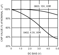 Figure 27. Typical Variation In Capacitance vs DC Bias
The value of the ceramic capacitor can vary with temperature. The capacitor type X7R, which operates over a temperature range of –55°C to 125°C, will only vary the capacitance to within ±15%. The capacitor type X5R has a similar tolerance over a reduced temperature range of –55°C to 85°C. Many large value ceramic capacitors, larger than 1 µF are manufactured with Z5U or Y5V temperature characteristics. Their capacitance can drop by more than 50% as the temperature varies from 25°C to 85°C. Therefore, X7R and X5R types are recommended over Z5U and Y5V in applications where the ambient temperature will change significantly above or below 25°C.
Tantalum capacitors are less desirable than ceramic for use as output capacitors because they are more costly when comparing equivalent capacitance and voltage ratings in the 0.47-µF to 4.7-µF range.
Another important consideration is that tantalum capacitors have higher ESR values than equivalent size ceramics. This means that while it may be possible to find a tantalum capacitor with an ESR value within the stable range, it would have to be larger in capacitance (which means bigger and more costly) than a ceramic capacitor with the same ESR value. It should also be noted that the ESR of a typical tantalum will increase about 2:1 as the temperature goes from 25°C down to –40°C, so some guard band must be allowed.
9.2.2.7 RFI/EMI Susceptibility
RFI (radio frequency interference) and EMI (electromagnetic interference) can degrade any integrated circuit’s performance because of the small dimensions of the geometries inside the device. In applications where circuit sources are present which generate signals with significant high frequency energy content (> 1 MHz), care must be taken to ensure that this does not affect the IC regulator.
If RFI/EMI noise is present on the input side of the regulator (such as applications where the input source comes from the output of a switching regulator), good ceramic bypass capacitors must be used at the input pin of the IC.
If a load is connected to the IC output which switches at high speed (such as a clock), the high-frequency current pulses required by the load must be supplied by the capacitors on the IC output. Because the bandwidth of the regulator loop is less than 100 kHz, the control circuitry cannot respond to load changes above that frequency. This means the effective output impedance of the IC at frequencies above 100 kHz is determined only by the output capacitors.
In applications where the load is switching at high speed, the output of the IC may need RF isolation from the load. It is recommended that some inductance be placed between the output capacitor and the load, and good RF bypass capacitors be placed directly across the load.
PCB layout is also critical in high noise environments, because RFI/EMI is easily radiated directly into PC traces. Noisy circuitry should be isolated from clean circuits where possible, and grounded through a separate path. At MHz frequencies, ground planes begin to look inductive and RFI/ EMI can cause ground bounce across the ground plane. In multi-layer PCB applications, care should be taken in layout so that noisy power and ground planes do not radiate directly into adjacent layers which carry analog power and ground.
9.2.2.8 Output Noise
Noise is specified in two ways: Spot Noise or Output Noise Density is the RMS sum of all noise sources, measured at the regulator output, at a specific frequency (measured with a 1Hz bandwidth). This type of noise is usually plotted on a curve as a function of frequency. Total Output Noise or Broad-Band Noise is the RMS sum of spot noise over a specified bandwidth, usually several decades of frequencies.
Attention should be paid to the units of measurement. Spot noise is measured in units µV/root-Hz or nV/root-Hz and total output noise is measured in µV(rms).
The primary source of noise in low-dropout regulators is the internal reference. Noise can be reduced in two ways: by increasing the transistor area or by increasing the current drawn by the internal reference. Increasing the area will decrease the chance of fitting the die into a smaller package. Increasing the current drawn by the internal reference increases the total supply current (ground pin current).
9.2.3 Application Curves
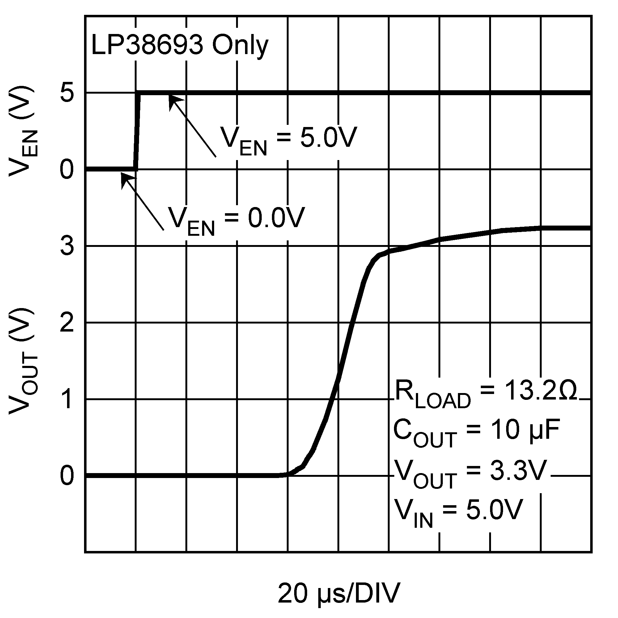 Figure 28. VOUT vs VEN, ON (LP38693 Only)
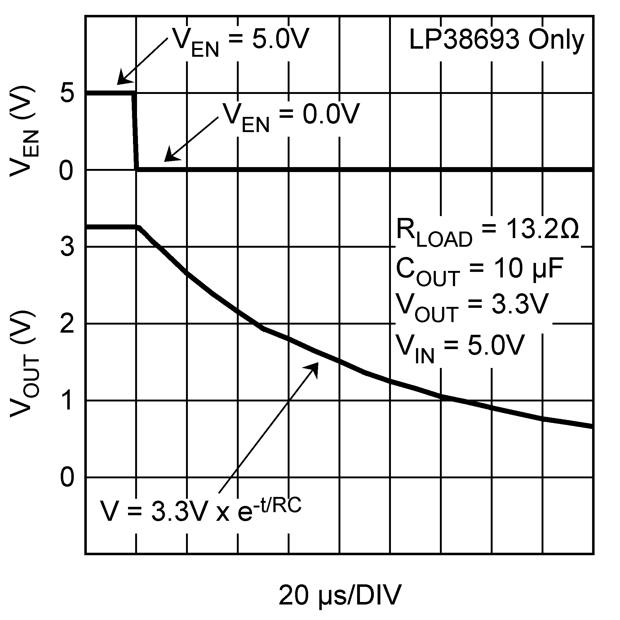 Figure 29. VOUT vs VEN, OFF (LP38693 Only)