ZHCS589D May 2005 – February 2015 LP3878-ADJ
PRODUCTION DATA.
- 1 特性
- 2 应用
- 3 说明
- 4 修订历史记录
- 5 Pin Configuration and Functions
- 6 Specifications
- 7 Detailed Description
- 8 Application and Implementation
- 9 Power Supply Recommendations
- 10Layout
- 11器件和文档支持
- 12机械、封装和可订购信息
6 Specifications
6.1 Absolute Maximum Ratings
over operating free-air temperature range (unless otherwise noted)(1)(2)| MIN | MAX | UNIT | |
|---|---|---|---|
| SHUTDOWN pin | 1 | kV | |
| Power dissipation(3) | Internally Limited | ||
| Input supply voltage (survival), VIN | −0.3 | 16 | V |
| ADJ pin | −0.3 | 6 | V |
| Output voltage (survival), VOUT(4) | −0.3 | 6 | V |
| IOUT (survival) | Short-Circuit Protected | ||
| Input – output voltage (survival), VIN – VOUT(5) | −0.3 | 16 | V |
| Storage temperature, Tstg | –65 | 150 | °C |
(1) Stresses beyond those listed under Absolute Maximum Ratings may cause permanent damage to the device. These are stress ratings only, which do not imply functional operation of the device at these or any other conditions beyond those indicated under Recommended Operating Conditions. Exposure to absolute-maximum-rated conditions for extended periods may affect device reliability.
(2) If Military- or Aerospace-specified devices are required, please contact the TI Sales Office/Distributors for availability and specifications.
(3) The maximum allowable power dissipation is a function of the maximum junction temperature, TJ(MAX), the junction-to-ambient thermal resistance, RθJA, and the ambient temperature, TA. The maximum allowable power dissipation at any ambient temperature is calculated using: P(MAX) = (TJ(MAX) – TA) / RθJA. The value of RθJA for the WSON (NGT) and SO PowerPAD (DDA) packages are specifically dependent on PCB trace area, trace material, and the number of layers and thermal vias. For improved thermal resistance and power dissipation for the WSON package, see Application Note AN-1187, SNOA401. Exceeding the maximum allowable power dissipation will cause excessive die temperature, and the regulator will go into thermal shutdown.
(4) If used in a dual-supply system where the regulator load is returned to a negative supply, the LP3878-ADJ output must be diode-clamped to ground.
(5) The PNP pass element contains a parasitic diode between the IN pin and the OUT pin that is normally reverse-biased. Forcing the OUT pin voltage above the IN pin voltage will turn on this diode and may induce a latch-up mode which can damage the part (see Application and Implementation).
6.2 ESD Ratings
| VALUE | UNIT | |||
|---|---|---|---|---|
| V(ESD) | Electrostatic discharge | Human body model (HBM), per ANSI/ESDA/JEDEC JS-001, all pins(1) | ±2000 | V |
(1) JEDEC document JEP155 states that 500-V HBM allows safe manufacturing with a standard ESD control process.
6.3 Recommended Operating Conditions
over operating free-air temperature range (unless otherwise noted)| MIN | MAX | UNIT | ||
|---|---|---|---|---|
| VIN | Supply input voltage | 2.5 | 16 | V |
| VSD | SHUTDOWN input voltage | VIN | V | |
| IOUT | Output current | 800 | mA | |
| TJ | Operating junction temperature | −40 | 125 | °C |
6.4 Thermal Information
| THERMAL METRIC(1) | LP3878-ADJ | UNIT | ||
|---|---|---|---|---|
| DDA | NGT | |||
| 8 PINS | ||||
| RθJA | Junction-to-ambient thermal resistance | 42.5 | 38.1 | °C/W |
| RθJC(top) | Junction-to-case (top) thermal resistance | 54.0 | 27.9 | |
| RθJB | Junction-to-board thermal resistance | 26.5 | 15.2 | |
| ψJT | Junction-to-top characterization parameter | 8.0 | 0.2 | |
| ψJB | Junction-to-board characterization parameter | 26.4 | 15.3 | |
| RθJC(bot) | Junction-to-case (bottom) thermal resistance | 3.6 | 4.5 | |
(1) For more information about traditional and new thermal metrics, see the IC Package Thermal Metrics application report, SPRA953.
6.5 Electrical Characteristics
Limits are specified through design, testing, or correlation. The limits are used to calculate TI's Average Outgoing Quality Level (AOQL). Unless otherwise specified: TJ = 25°C, VIN = 3 V, VOUT = 1 V, IOUT = 1 mA, COUT = 10 µF, CIN = 4.7 µF, VSD = 2 VVSD, CBYPASS = 10 nF.| PARAMETER | TEST CONDITIONS | MIN | TYP | MAX | UNIT | |
|---|---|---|---|---|---|---|
| VADJ | Adjust pin voltage | 0.99 | 1.00 | 1.01 | V | |
| 1 mA ≤ IOUT ≤ 800 mA, 3 V ≤ VIN ≤ 6 V | 0.98 | 1.00 | 1.02 | |||
| 1 mA ≤ IOUT ≤ 800 mA, 3 V ≤ VIN ≤ 6 V –40°C ≤ TJ ≤ 125°C |
0.97 | 1.03 | ||||
| ΔVOUT/ΔVIN | Output voltage line regulation | 3 V ≤ VIN ≤ 16 V | 0.007 | 0.014 | %/V | |
| 3 V ≤ VIN ≤ 16 V, –40°C ≤ TJ ≤ 125°C | 0.032 | |||||
| VIN(MIN) | Minimum input voltage required to maintain output regulation | IOUT = 800 mA, VOUT ≥ VOUT(NOM) – 1% | 2.5 | V | ||
| IOUT = 800 mA, VOUT ≥ VOUT(NOM) – 1% –40°C ≤ TJ ≤ 125°C |
3.1 | |||||
| IOUT = 800 mA, VOUT ≥ VOUT(NOM) – 1% 0 ≤ TJ ≤ 125°C |
2.5 | |||||
| IOUT = 800 mA, VOUT ≥ VOUT(NOM) – 1% 0 ≤ TJ ≤ 125°C, –40°C ≤ TJ ≤ 125°C |
2.8 | |||||
| IOUT = 750 mA, VOUT ≥ VOUT(NOM) – 1% | 2.5 | |||||
| IOUT = 750 mA, VOUT ≥ VOUT(NOM) – 1% –40°C ≤ TJ ≤ 125°C |
3.0 | |||||
| VDOUT | Dropout voltage(1)
VOUT = 3.8 V |
IOUT = 100 µA | 1 | 2 | mV | |
| IOUT = 100 µA, –40°C ≤ TJ ≤ 125°C | 3 | |||||
| IOUT = 200 mA | 150 | 200 | ||||
| IOUT = 200 mA, –40°C ≤ TJ ≤ 125°C | 300 | |||||
| IOUT = 800 mA | 475 | 600 | ||||
| IOUT = 800 mA, –40°C ≤ TJ ≤ 125°C | 1100 | |||||
| IGND | Ground pin current | IOUT = 100 µA | 180 | 200 | µA | |
| IOUT = 100 µA, –40°C ≤ TJ ≤ 125°C | 225 | |||||
| IOUT = 200 mA | 1.5 | 2 | mA | |||
| IOUT = 200 mA, –40°C ≤ TJ ≤ 125°C | 3.5 | |||||
| IOUT = 800 mA | 5.5 | 8.5 | ||||
| IOUT = 800 mA, –40°C ≤ TJ ≤ 125°C | 15 | |||||
| IOUT(PK) | Peak output current | VOUT ≥ VOUT(NOM) − 5% | 1200 | mA | ||
| IOUT(MAX) | Short-circuit current | RL = 0 Ω (steady state) | 1300 | |||
| en | Output noise voltage (RMS) | Bandwidth = 100 Hz to 100 kHz, CBYPASS = 10 nF | 18 | µV(RMS) | ||
| ΔVOUT/ΔVIN | Ripple rejection | f = 1 kHz | 60 | dB | ||
| IADJ | ADJ pin bias current (sourcing) | IOUT = 800 mA | 200 | nA | ||
| SHUTDOWN Input | ||||||
| VSD | SHUTDOWN input voltage | VH = Output ON | 1.4 | V | ||
| VH = Output ON, –40°C ≤ TJ ≤ 125°C | 1.6 | |||||
| VL = Output OFF, IIN ≤ 10 µA | 0.20 | |||||
| VL = Output OFF, IIN ≤ 10 µA –40°C ≤ TJ ≤ 125°C |
0.04 | |||||
| VOUT ≤ 10 mV, IIN ≤ 50 µA | 0.6 | |||||
| ISD | SHUTDOWN input current | VSD = 0 V | 0.02 | µA | ||
| VSD = 0 V, –40°C ≤ TJ ≤ 125°C | −1 | |||||
| VSD = 5 V | 5 | |||||
| VSD = 5 V, –40°C ≤ TJ ≤ 125°C | 15 | |||||
(1) Dropout voltage specification applies only if VIN is sufficient so that it does not limit regulator operation.
6.6 Typical Characteristics
Unless otherwise specified: VIN = 3.3 V, VOUT = 1 V, IOUT = 1 mA, CIN = 4.7 µF, COUT = 10 µF, VSD = 2 V, CBYP = 10 nF, TJ = 25°C.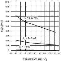 Figure 1. IGND vs Temperature
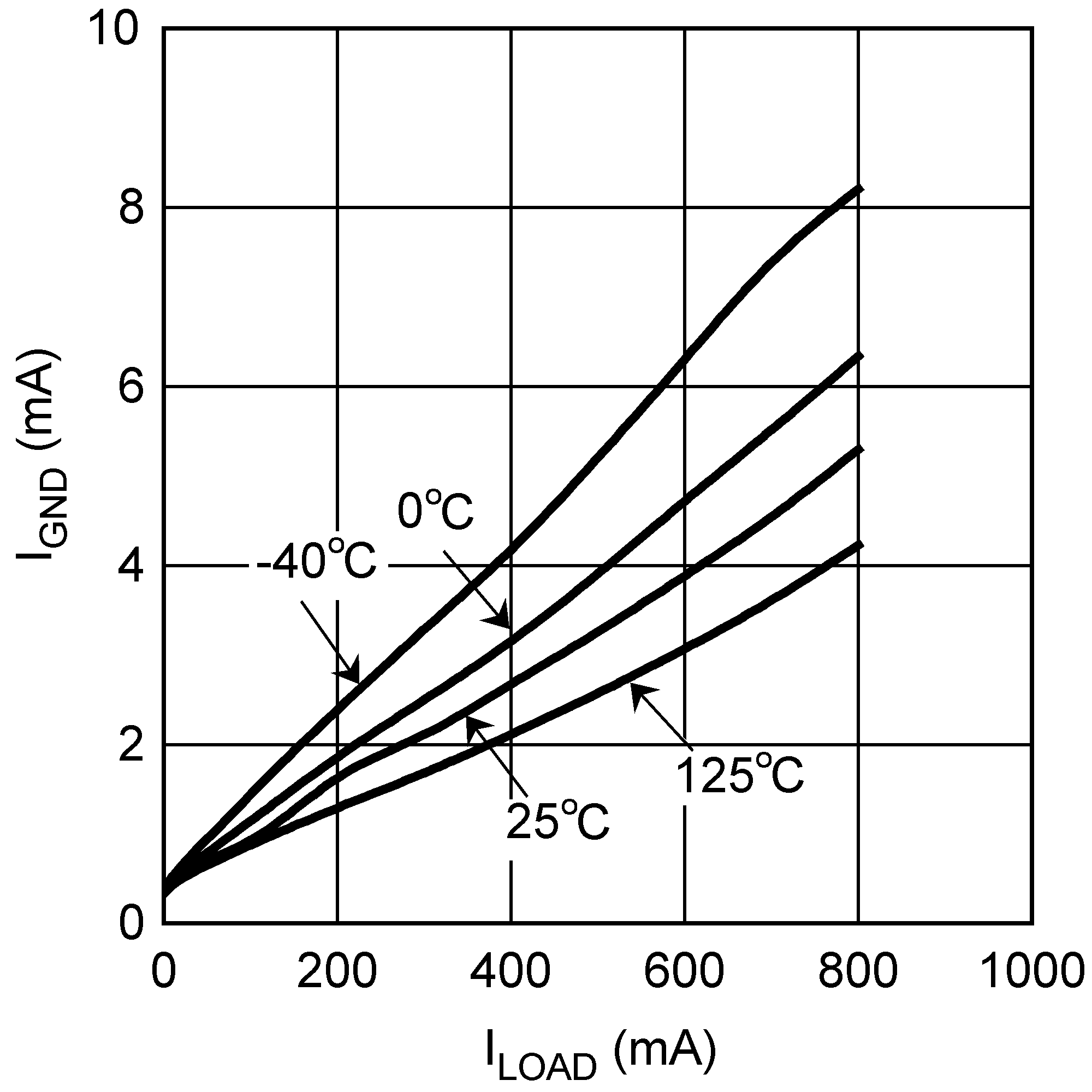 Figure 3. IGND vs ILoad
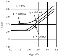 Figure 5. Minimum VIN vs VOUT
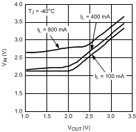 Figure 7. Minimum VIN vs VOUT
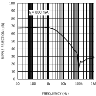 Figure 9. Ripple Rejection
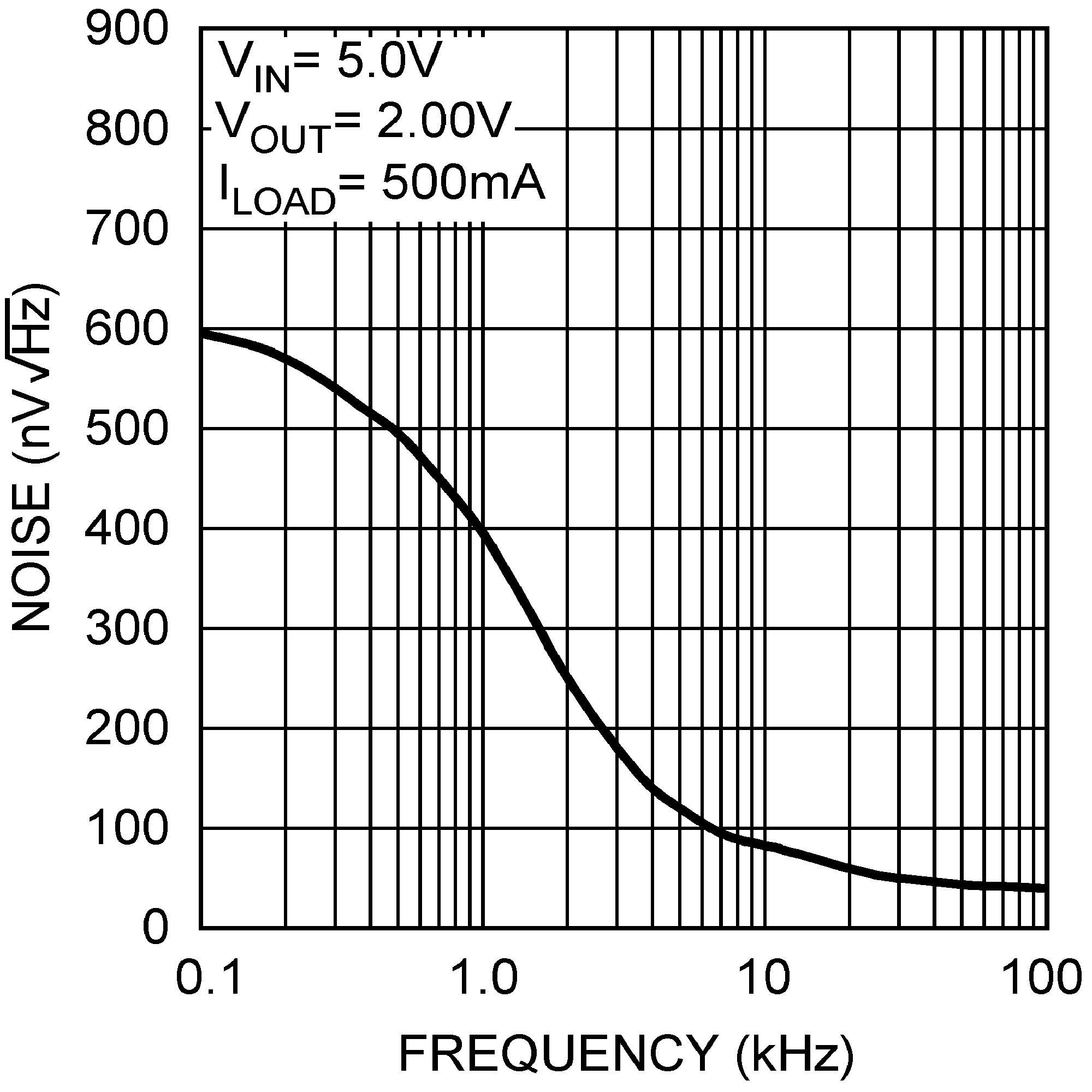 Figure 11. Output Noise Spectral Density
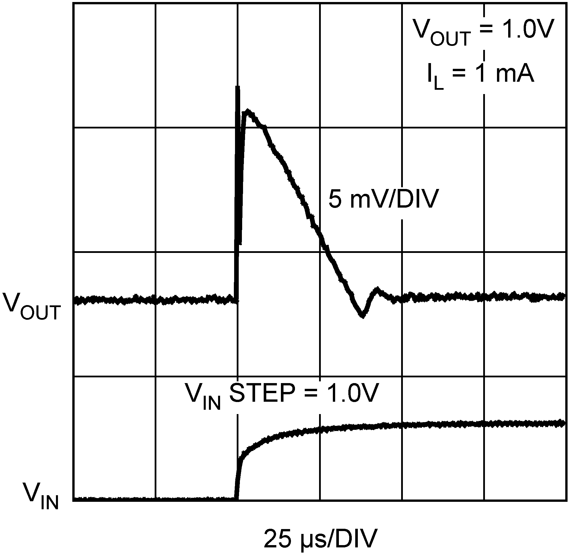 Figure 13. Line Transient Response
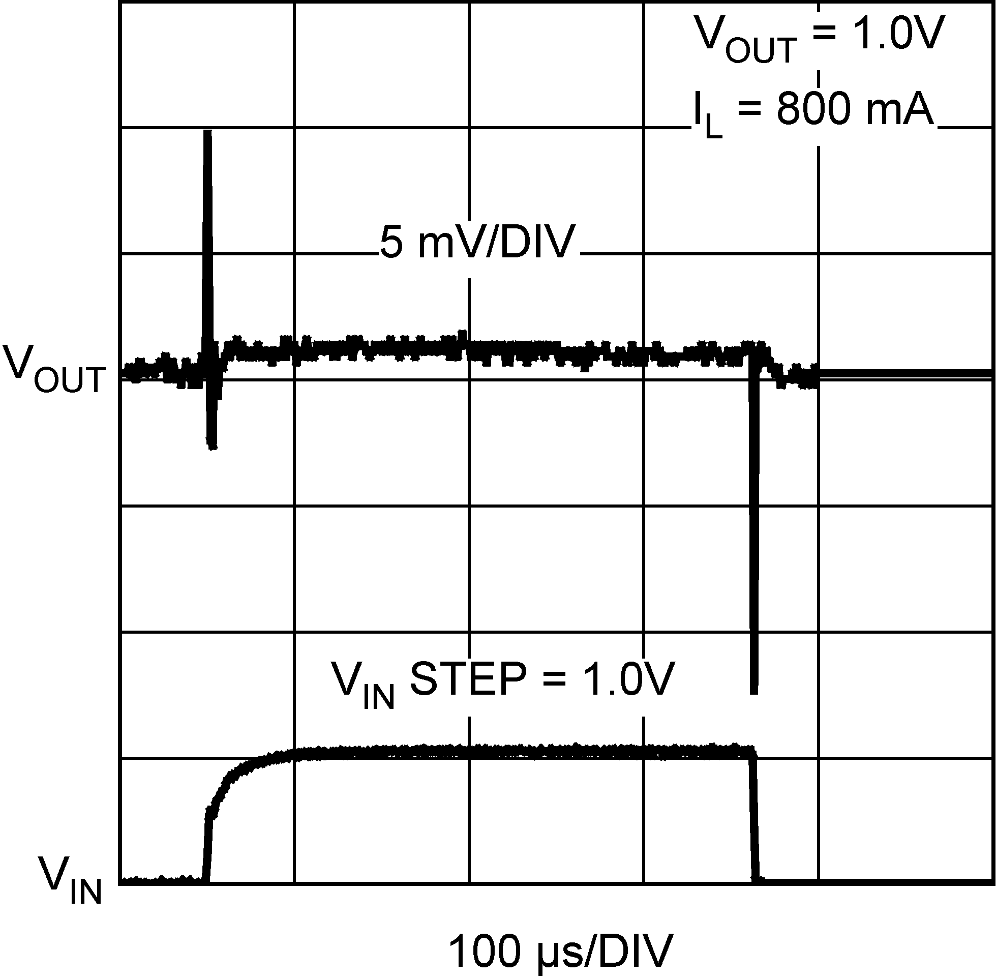 Figure 15. Line Transient Response
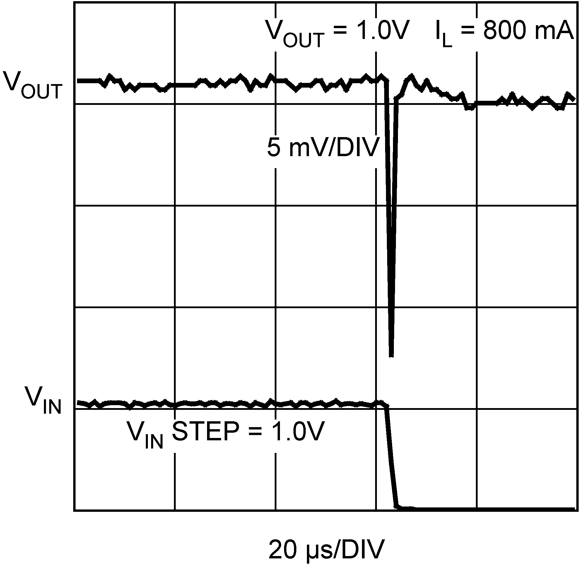 Figure 17. Line Transient Response
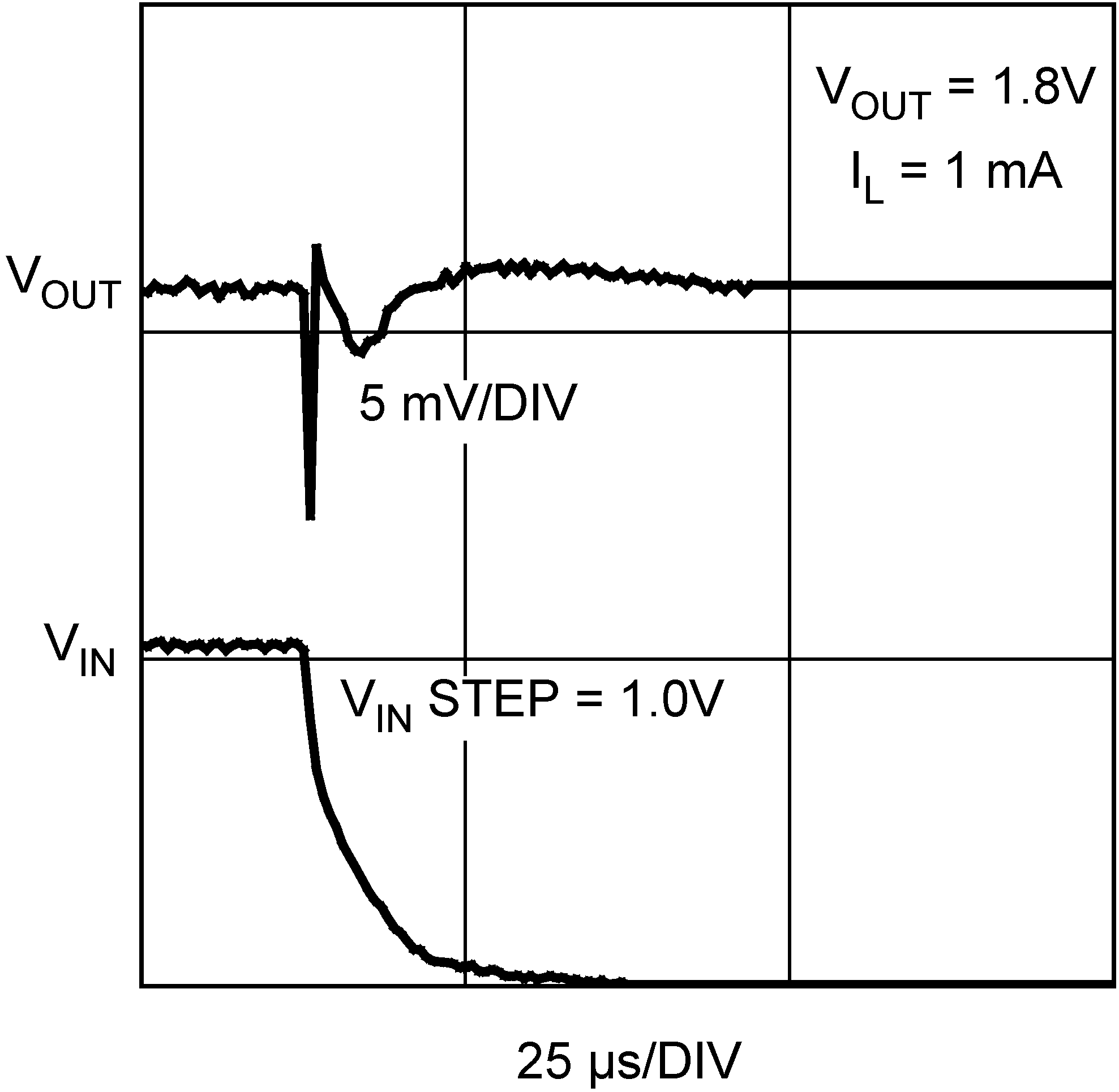 Figure 19. Line Transient Response
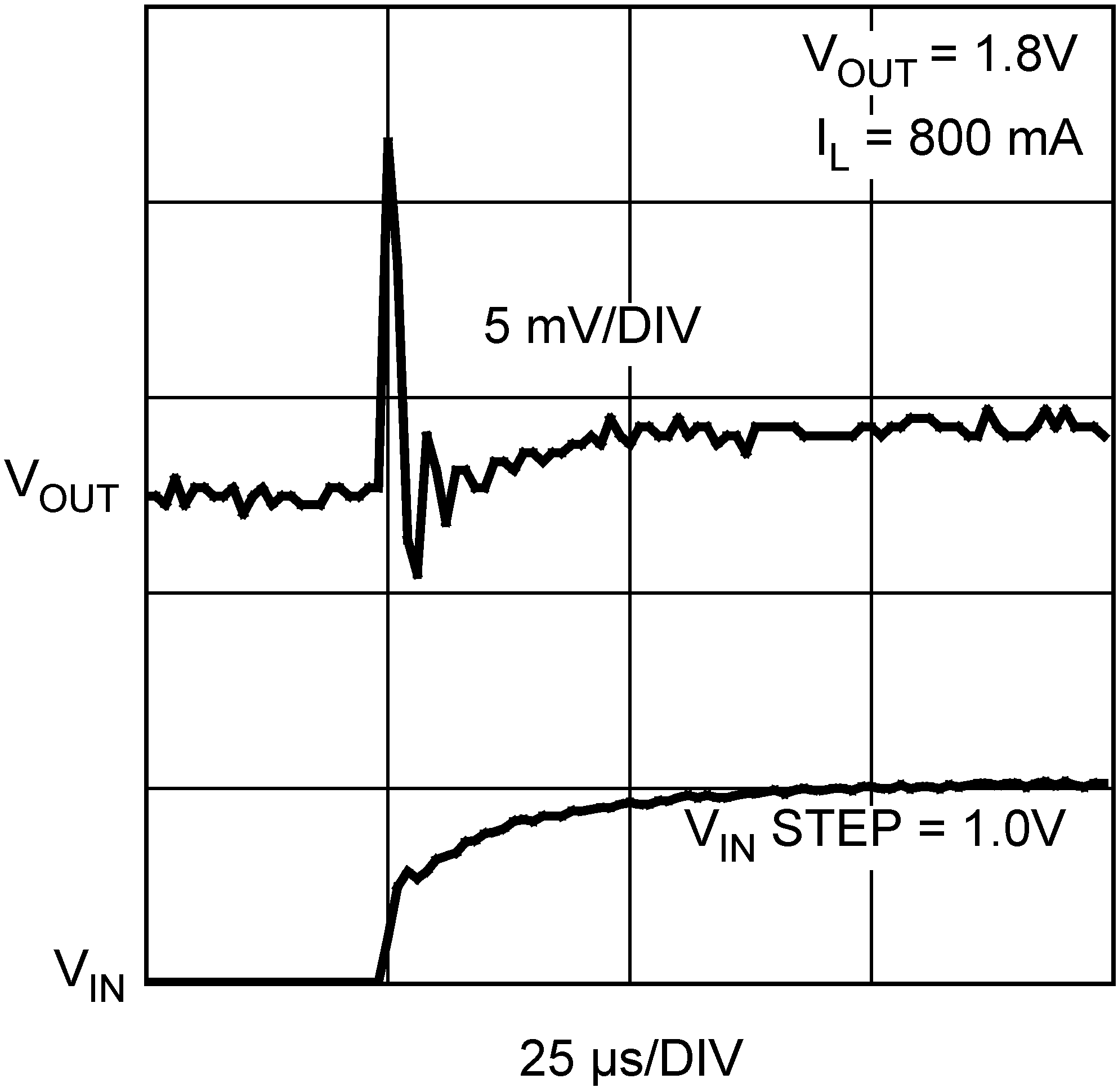 Figure 21. Line Transient Response
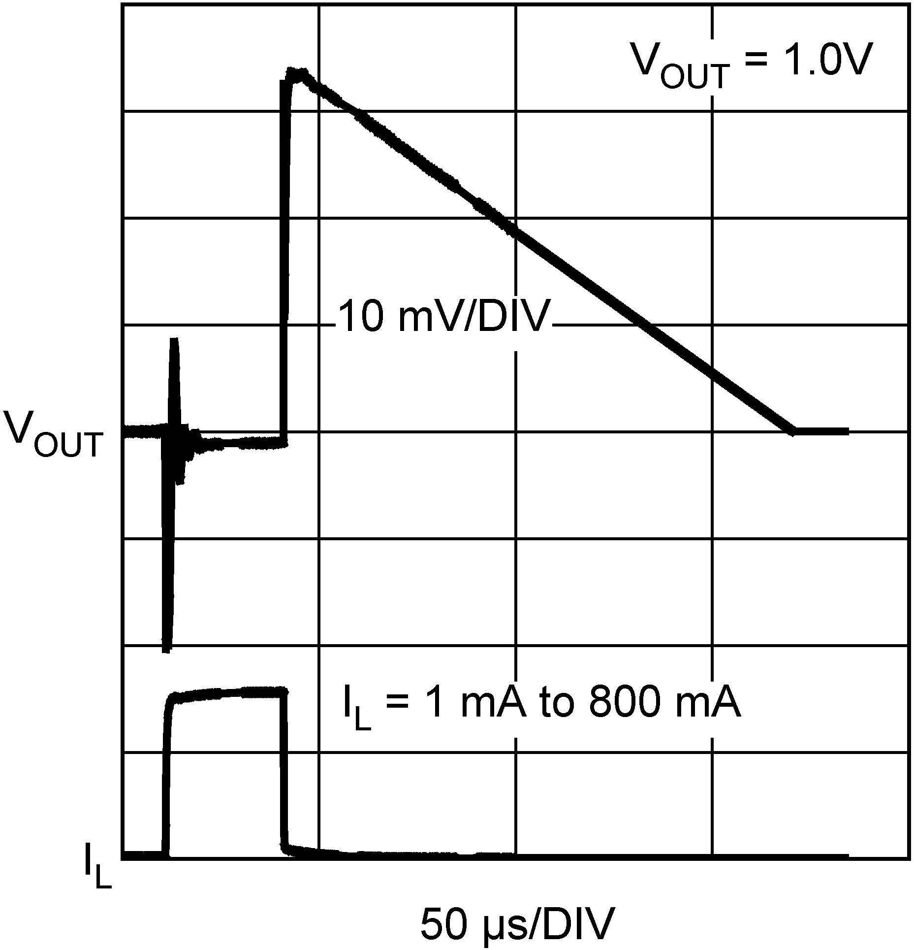 Figure 23. Load Transient Response
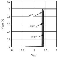 Figure 25. Turnon Characteristics
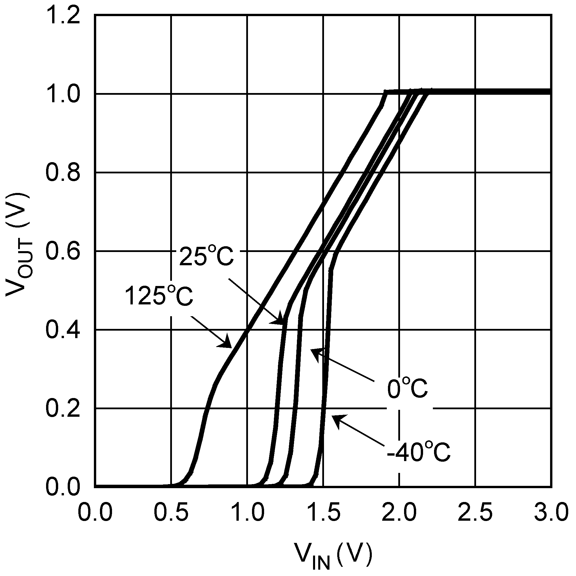 Figure 2. Minimum VIN Over Temperature
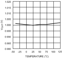 Figure 4. VOUT vs Temperature
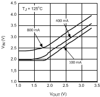 Figure 6. Minimum VIN vs VOUT
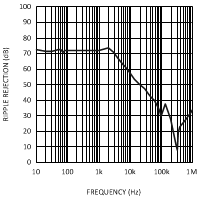 Figure 8. Ripple Rejection
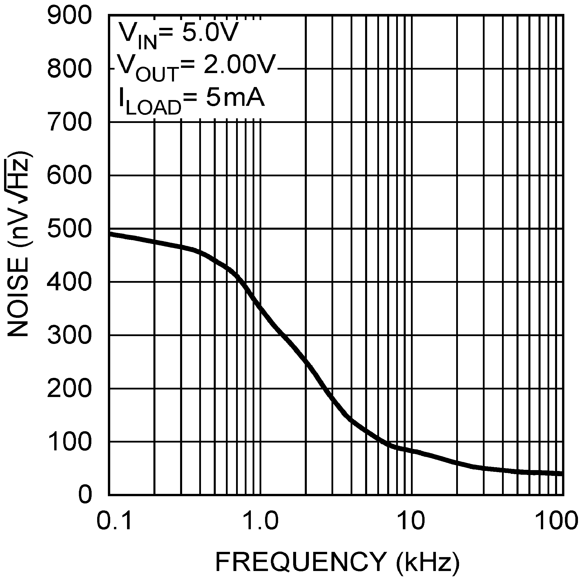 Figure 10. Output Noise Spectral Density
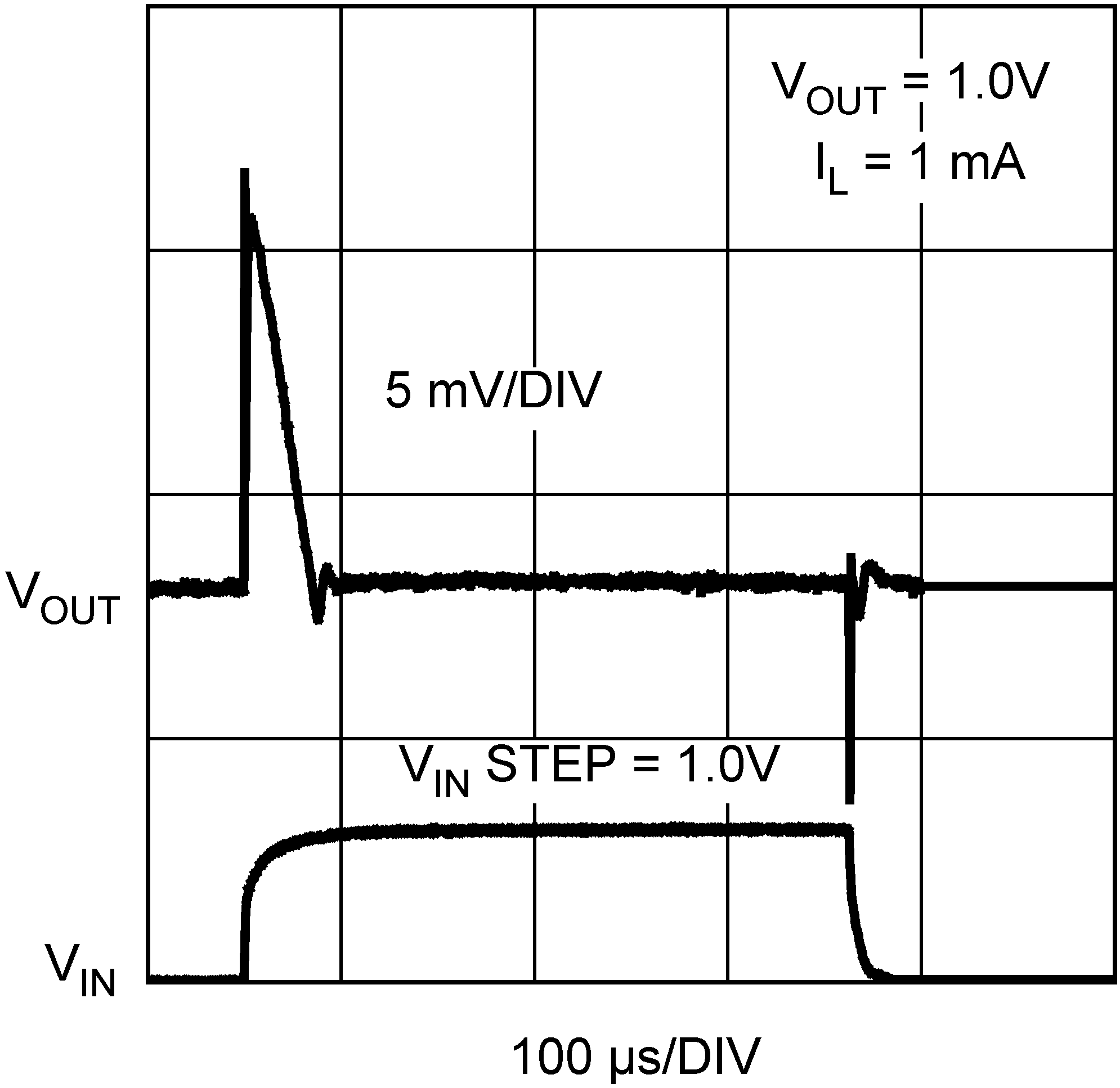 Figure 12. Line Transient Response
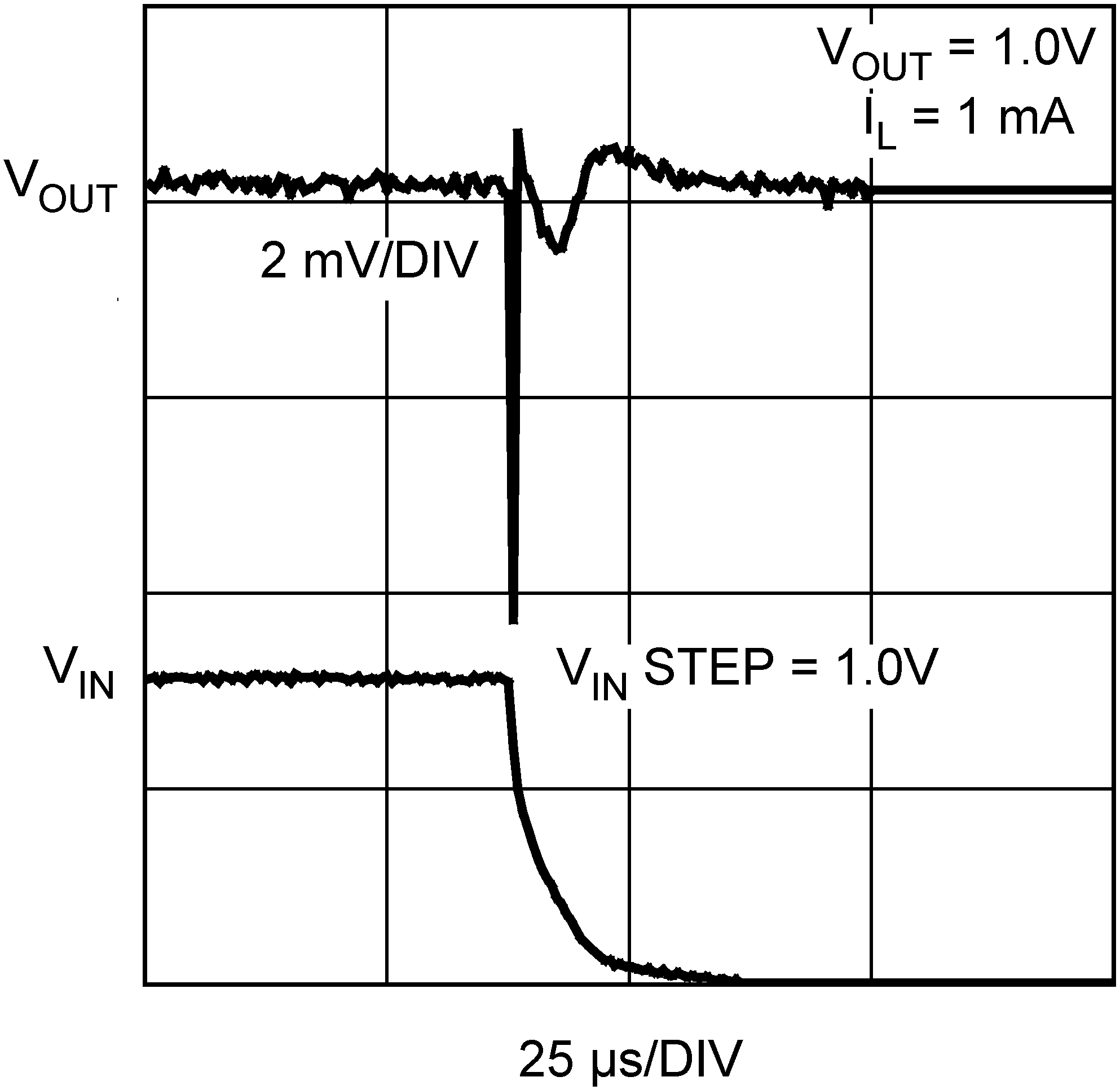 Figure 14. Line Transient Response
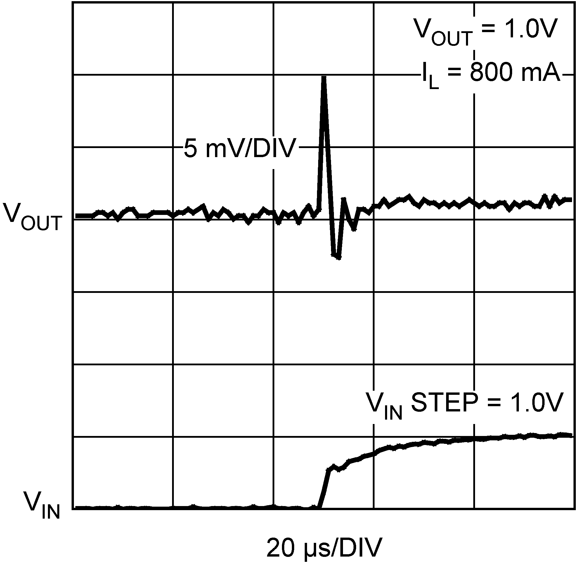 Figure 16. Line Transient Response
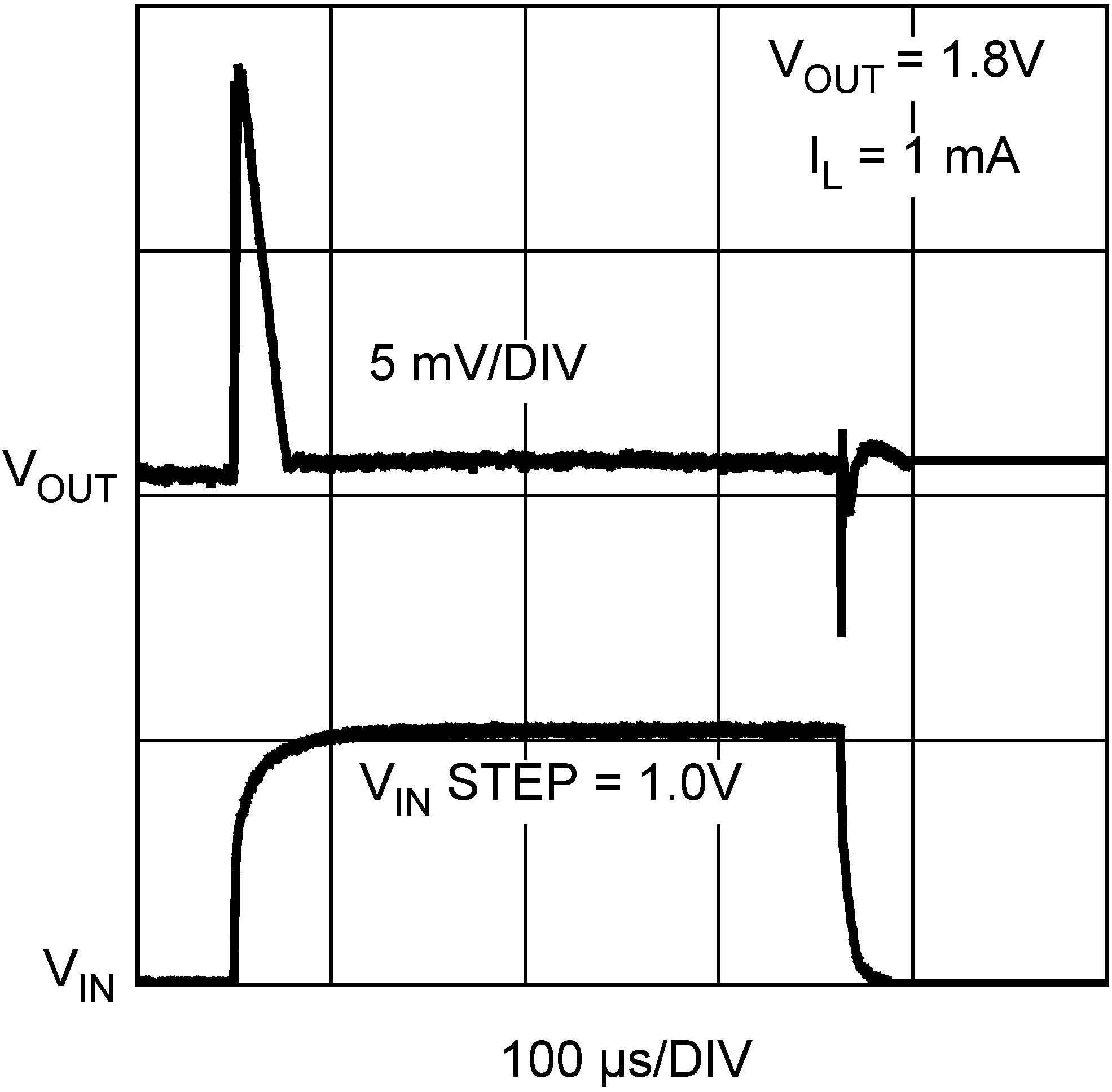 Figure 18. Line Transient Response
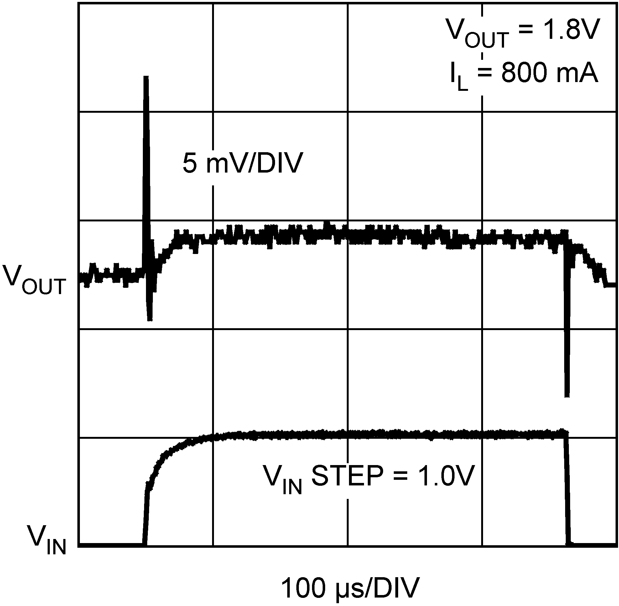 Figure 20. Line Transient Response
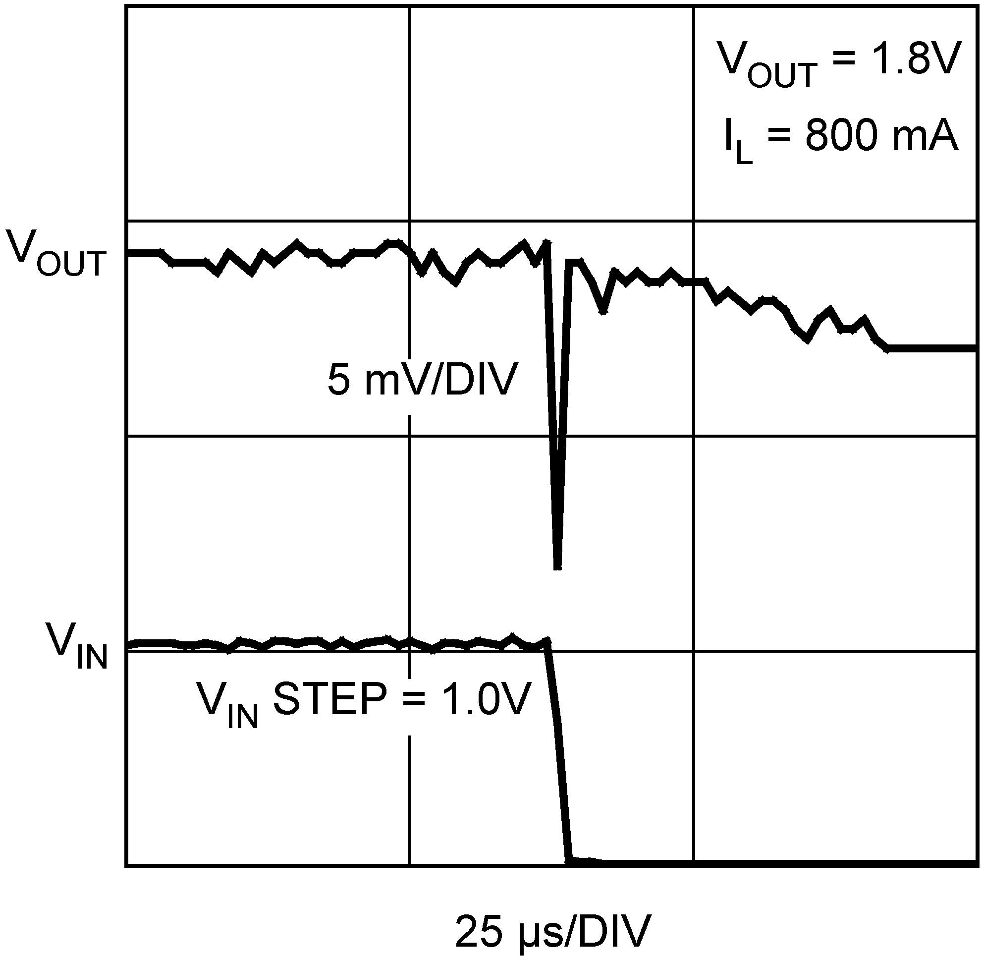 Figure 22. Line Transient Response
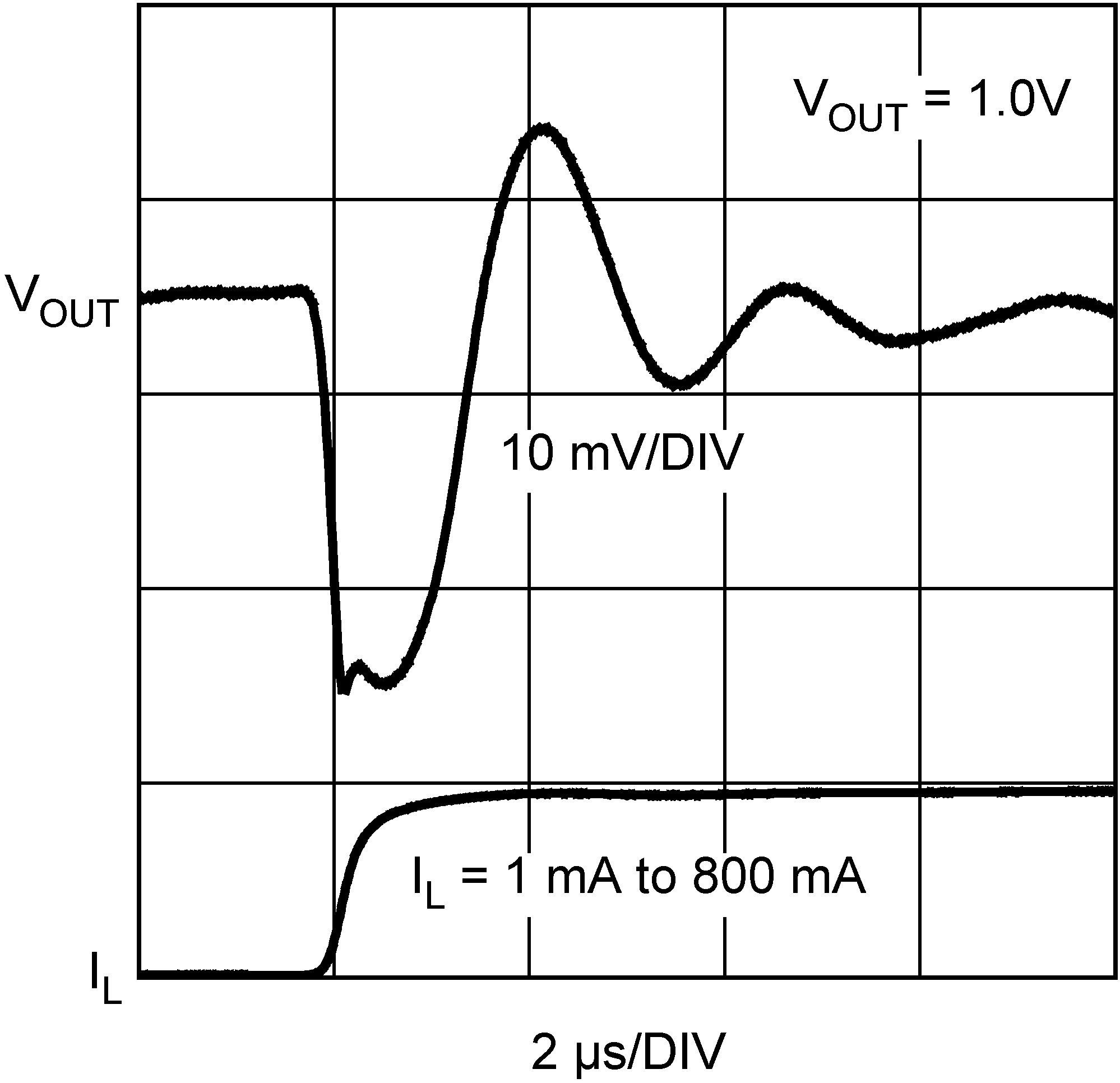 Figure 24. Load Transient Response
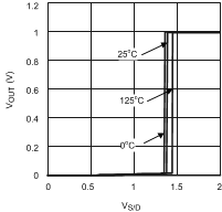 Figure 26. Turnoff Characteristics