SNVS185F February 2002 – April 2017 LP3982
PRODUCTION DATA.
- 1 Features
- 2 Applications
- 3 Description
- 4 Revision History
- 5 Pin Configuration and Functions
- 6 Specifications
- 7 Detailed Description
- 8 Application and Implementation
- 9 Power Supply Recommendations
- 10Layout
- 11Device and Documentation Support
- 12Mechanical, Packaging, and Orderable Information
8 Application and Implementation
NOTE
Information in the following applications sections is not part of the TI component specification, and TI does not warrant its accuracy or completeness. TI’s customers are responsible for determining suitability of components for their purposes. Customers should validate and test their design implementation to confirm system functionality.
8.1 Application Information
The LP3982 can provide 300-mA output current with 2.5-V to 6-V input. It is stable with a 2.2-μF ceramic output capacitor. An optional external bypass capacitor reduces the output noise without slowing down the load transient response. Typical output noise is 37 μVRMS at frequencies from 10 Hz to 100 kHz. Typical PSSR is
60 dB at 1 kHz.
8.2 Typical Application
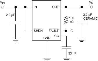 Figure 14. LP3982 Typical Application (Fixed VOUT Version)
8.2.1 Design Requirements
For typical ultra low-dropout CMOS-regulator applications, use the parameters listed in Table 1.
Table 1. Design Parameters
| DESIGN PARAMETER | EXAMPLE VALUE |
|---|---|
| Minimum input voltage | VOUT + 0.5 V |
| Nominal output voltage | 3.3 V |
| Maximum output current | 300 mA |
| RMS noise, 10 Hz to 100 kHz | 37 µVRMS |
| PSRR at 1 kHz | 60 dB |
8.2.2 Detailed Design Procedure
8.2.2.1 Custom Design With WEBENCH® Tools
Click here to create a custom design using the LP3982 device with the WEBENCH® Power Designer.
- Start by entering the input voltage (VIN), output voltage (VOUT), and output current (IOUT) requirements.
- Optimize the design for key parameters such as efficiency, footprint, and cost using the optimizer dial.
- Compare the generated design with other possible solutions from Texas Instruments.
The WEBENCH Power Designer provides a customized schematic along with a list of materials with real-time pricing and component availability.
In most cases, these actions are available:
- Run electrical simulations to see important waveforms and circuit performance
- Run thermal simulations to understand board thermal performance
- Export customized schematic and layout into popular CAD formats
- Print PDF reports for the design, and share the design with colleagues
Get more information about WEBENCH tools at www.ti.com/WEBENCH.
8.2.2.2 Output Voltage Setting (ADJ Version Only)
The output voltage is set according to the amount of negative feedback (the pass transistor inverts the feedback signal.) Figure 15 simplifies the topology of the LP3982. This type of regulator can be represented as an op amp configured as non-inverting amplifier and a fixed DC Voltage (VREF) for its input signal. The special characteristic of this op amp is its extra-large output transistor that only sources current. In terms of its non-inverting configuration, the output voltage equals VREF times the closed loop gain:

Use Equation 6 for adjusting the output to a particular voltage:

Choose R2 = 100 kΩ to optimize accuracy, power supply rejection, noise, and power consumption.
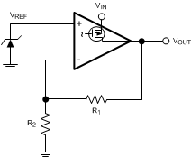 Figure 15. Regulator Topology Simplified
Similarity in the output capabilities exists between op amps and linear regulators. Just as rail-to-rail output op amps allow their output voltage to approach the supply voltage, low dropout regulators (LDOs) allow their output voltage to operate close to the input voltage. Both achieve this by the configuration of their output transistors. Standard operational amplifiers and regulator outputs are at the source (or emitter) of the output transistor. Rail-to-rail op amp and LDO regulator outputs are at the drain (or collector) of the output transistor. This replaces the threshold (or diode drop) limitations on the output with the less restrictive source-to-drain (or VSAT) limitations. There is a trade-off; the output impedance become significantly higher, thus providing a critically lower pole when combined with the capacitive load. That is why rail-to-rail operational amplifiers are usually poor at driving capacitive loads and a series output resistor recommended when doing so. LDOs require the same series resistance except that the internal resistance of the output capacitor will usually suffice. Refer to the Output Capacitance section for more information.
8.2.2.3 Output Capacitance
The LP3982 is specifically designed to employ ceramic output capacitors as low as 2.2 μF. Ceramic capacitors below 10 μF offer significant cost and space savings, along with high frequency noise filtering. Higher values and other types and of capacitor may be used, but their equivalent series resistance (ESR) must be maintained below 0.5 Ω.
Ceramic capacitor of the value required by the LP3982 are available in the following dielectric types: Z5U, Y5V, X5R, and X7R. The Z5U and Y5V types exhibit a 50% or more drop in capacitance value as their temperature increases from 25°C, an important consideration. The X5R generally maintain their capacitance value within ±20%. The X7R type are desirable for their tighter tolerance of 10% over temperature.
Ceramic capacitors pose a challenge because of their relatively low ESR. Like most other LDOs, the LP3982 relies on a zero in the frequency response to compensate against excessive phase shift in the feedback loop of the regulator. If the phase shift reaches 360° (that is, becomes positive), the regulator oscillates. This compensation usually resides in the zero generated by the combination of the output capacitor with its ESR. The zero is intended to cancel the effects of the pole generated by the load capacitance (CL) combined with the parallel combination of the load resistance (RL) and the output resistance (RO) of the regulator. The challenge posed by low ESR capacitors is that the zero it generates can be too high in frequency for the pole it is intended to compensate. The LP3982 overcomes this challenge by internally generating a strategically placed zero.
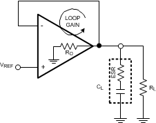 Figure 16. Simplified Model of Regulator Loop Gain Components
Figure 16 shows a basic model for the linear regulator that helps describe what happens to the output signal as it is processed through its feedback loop; that is, describe its loop gain (LG). The LG includes two main transfer functions: the error amplifier and the load. The error amplifier provides voltage gain and a dominant pole, while the load provides a zero and a pole. The LG of the model in Figure 16 is described by Equation 7:

The first term of Equation 7 expresses the voltage gain (numerator) and a single pole role-off (denominator) of the error amplifier. The second term expresses the zero (numerator) and pole (denominator) of the load in combination with the RO of the regulator.
Figure 17 shows a Bode plot that represents a case where the zero contributed by the load is too high to cancel the effect of the pole contributed by the load and RO. The solid line represents the loop gain while the dashed line represents the corresponding phase shift. Notice that the phase shift at unity gain is a total 360°, the criteria for oscillation.
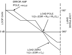 Figure 17. Loop Gain Bode Plot Illustrating Inadequately High Zero for Stability Compensation
The LP3982 generates an internal zero that makes up for the inadequately high zero of the low ESR ceramic output capacitor. This internally generated zero is strategically placed to provide positive phase shift near unity gain, thus providing a stable phase margin.
8.2.2.4 Input Capacitor
The LP3982 requires a minimum input capacitance of about 1 μF. The value may be increased indefinitely. The type is not critical to stability. However, instability may occur with bench set-ups where long supply leads are used, particularly at near dropout and high current conditions. This is attributed to the lead inductance coupling to the output through the gate oxide of the pass transistor; thus, forming a pseudo LCR network within the loop gain. A 10-μF tantalum input capacitor remedies this non-situ condition; its larger ESR acts to dampen the pseudo-LCR network. This may only be necessary for some bench setups. A 1-μF ceramic input capacitor are fine for most end-use applications.
If a tantalum input capacitor is intended for the final application, it is important to consider their tendency to fail in short circuit mode, thus potentially damaging the part.
8.2.2.5 Noise Bypass Capacitor
The noise bypass capacitor (CC) significantly reduces output noise of the LP3982. It connects between pin 6 and ground. The optimum value for CC is 33 nF.
Pin 6 directly connects to the high impedance output of the bandgap. The DC leakage of the CC capacitor must be considered; loading down the reference reduces the output voltage. NPO and COG ceramic capacitors typically offer very low leakage. Polypropylene and polycarbonate film carbonate capacitor offer even lower leakage currents.
CC does not affect the transient response; however, it does affect turnon time. The smaller the CC value, the faster the turnon time.
8.2.2.6 Fault Detection
The LP3982 provides a FAULT pin that goes low during out of regulation conditions like current limit and thermal shutdown, or when it approaches dropout. The latter monitors the input-to-output voltage differential and compares it against a threshold that is slightly above the dropout voltage. This threshold also tracks the dropout voltage as it varies with load current. Refer to Figure 3 in the Typical Characteristics section.
The FAULT pin requires a pullup resistor because it is an open-drain output. This resistor must be large in value to reduce energy drain. A 100-kΩ pullup resistor works well for most applications.
Figure 18 shows the LP3982 with delay added to the FAULT pin for the reset pin of a microprocessor. The output of the comparator stays low for a preset amount of time after the regulator comes out of a fault condition.
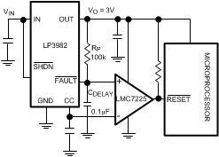 Figure 18. Power-On Delayed Reset Application
The delay time for the application of Figure 18 is set by Equation 8:

The application is set for a reset delay time of 8.8 ms. The comparator must have high impedance inputs so as to not load down the VREF at the CC pin of the LP3982.
8.2.2.7 Power Dissipation
Knowing the device power dissipation and proper sizing of the thermal plane connected to the tab or pad is critical to ensuring reliable operation. Device power dissipation depends on input voltage, output voltage, and load conditions and can be calculated with Equation 9:
Power dissipation can be minimized, and greater efficiency can be achieved, by using the lowest available voltage drop option that would still be greater than the dropout voltage (VDO). However, keep in mind that higher voltage drops result in better dynamic (that is, PSRR and transient) performance. On the WSON (NGM) package, the primary conduction path for heat is through the exposed power pad to the PCB. To ensure the device does not overheat, connect the exposed pad, through thermal vias, to an internal ground plane with an appropriate amount of copper PCB area. On the VSSOP (DGK) package, the primary conduction path for heat is through the pins to the PCB. The maximum allowable junction temperature (TJ(MAX)) determines maximum power dissipation allowed (PD(MAX)) for the device package. Power dissipation and junction temperature are most often related by the junction-to-ambient thermal resistance (RθJA) of the combined PCB and device package and the temperature of the ambient air (TA), according to Equation 10 or Equation 11:
RθJA is highly dependent on the heat-spreading capability of the particular PCB design, and therefore varies according to the total copper area, copper weight, and location of the planes. The RθJA recorded in Thermal Information is determined by the specific EIA/JEDEC JESD51-7 standard for PCB and copper-spreading area, and is to be used only as a relative measure of package thermal performance. For a well-designed thermal layout, RθJA is the sum of the package junction-to-case (bottom) thermal resistance (RθJCbot) plus the thermal resistance contribution by the PCB copper area acting as a heat sink.
Improvements and absolute measurements of the RθJA can be estimated by utilizing the thermal shutdown circuitry that is internal to the device. The thermal shutdown turns off the pass transistor of the device when its junction temperature reaches 160°C (typical). The pass transistor does not turn on again until the junction temperature drops about 10°C (hysteresis).
Using the thermal shutdown circuit to estimate, RθJA can be as follows: with a low input-to-output voltage differential, set the load current to 300 mA. Increase the input voltage until the thermal shutdown begins to cycle on and off. Then slowly decrease VIN (100-mV increments) until the device stays on. Record the resulting voltage differential (VD) and use it in Equation 12:

8.2.2.8 Estimating Junction Temperature
The EIA/JEDEC standard recommends the use of psi (Ψ) thermal characteristics to estimate the junction temperatures of surface mount devices on a typical PCB board application. These characteristics are not true thermal resistance values, but rather package specific thermal characteristics that offer practical and relative means of estimating junction temperatures. These psi metrics are determined to be significantly independent of copper-spreading area. The key thermal characteristics (ΨJT and ΨJB) are given in Thermal Information and are used in accordance with Equation 13 or Equation 14.
where
- PD(MAX) is explained in Equation 9.
- TTOP is the temperature measured at the center-top of the device package.
where
- PD(MAX) is explained in Equation 9.
- TBOARD is the PCB surface temperature measured 1-mm from the device package and centered on the package edge.
For more information about the thermal characteristics ΨJT and ΨJB, see the TI Application Report Semiconductor and IC Package Thermal Metrics (SPRA953), available for download at www.ti.com.
For more information about measuring TTOP and TBOARD, see the TI Application Report Using New Thermal Metrics (SBVA025), available for download at www.ti.com.
For more information about the EIA/JEDEC JESD51 PCB used for validating RθJA, see the TI Application Report Thermal Characteristics of Linear and Logic Packages Using JEDEC PCB Designs (SZZA017), available for download at www.ti.com.
8.2.3 Application Curves
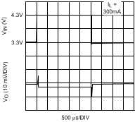 Figure 19. Line Transient Response
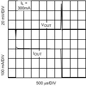 Figure 20. Load Transient