SNVS185F February 2002 – April 2017 LP3982
PRODUCTION DATA.
- 1 Features
- 2 Applications
- 3 Description
- 4 Revision History
- 5 Pin Configuration and Functions
- 6 Specifications
- 7 Detailed Description
- 8 Application and Implementation
- 9 Power Supply Recommendations
- 10Layout
- 11Device and Documentation Support
- 12Mechanical, Packaging, and Orderable Information
5 Pin Configuration and Functions
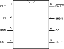
DGK Package
8-Pin VSSOP
Top View

The SET pin is internally disconnected for the fixed versions.
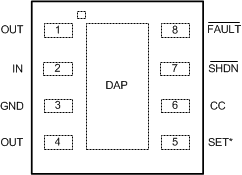
NGM Package
8-Pin WSON With Thermal Pad
Top View

The SET pin is internally disconnected for the fixed versions.
Pin Functions
| PIN | I/O | DESCRIPTION | |
|---|---|---|---|
| NAME | NO. | ||
| CC | 6 | — | Connect a capacitor between CC pin and ground to reduce the output noise. The optimum value for CC is 33 nF. |
| FAULT | 8 | Output | FAULT pin goes low during out of regulation conditions like current limit and thermal shutdown, or when it approaches dropout. Requires a pullup resistor because it is an active-low, open-drain output. |
| GND | 3 | Ground | Ground |
| IN | 2 | Input | This is the input supply voltage to the regulator. |
| OUT | 1, 4 | Output | Regulated output voltage |
| SET | 5 | Input | In the adjustable version a resistor divider connected to this pin sets the output voltage. The SET pin is internally disconnected for the fixed versions. |
| SHDN | 7 | Input | The SHDN pin allows the part to be turned to an ON or OFF state by pulling SHDN pin high or low. |
| DAP | √ | — | WSON Only - The DAP (Die Attached Pad) is an exposed pad that does not have an internal connection; it functions as a thermal relief when soldered to a copper plane. It is recommend that the DAP be connected to GND. See WSON Mounting section for more information. |