SNVS087AE October 2000 – May 2015 LP3985
PRODUCTION DATA.
- 1 Features
- 2 Applications
- 3 Description
- 4 Revision History
- 5 Pin Configuration and Functions
- 6 Specifications
- 7 Detailed Description
- 8 Application and Implementation
- 9 Power Supply Recommendations
- 10Layout
- 11Device and Documentation Support
- 12Mechanical, Packaging, and Orderable Information
7 Detailed Description
7.1 Overview
The LP3985 family of fixed-output, ultra-low-dropout and low noise regulators offers exceptional, cost-effective performance for battery powered applications. Available in output voltages from 2.5 V to 5 V, the family is capable of delivering 150-mA continuous load current. Standard regulator features, such as overcurrent and overtemperature protection, are also included.
The LP3985 contains several features to facilitate battery powered designs:
• Multiple voltage options
• Low dropout voltage, typical dropout of 60 mV at 150-mA load current
• Low quiescent current and low ground current, typically 140 μA at 150-mA load, and 85-μA at 0-mA load
• A shutdown feature is available, allowing the regulator to consume only 0.003 µA typically when the EN pin is pulled low
• Overtemperature protection and overcurrent protection circuitry is designed to safeguard the device during unexpected conditions
• Enhanced stability: The LP3985 is stable with output capacitor, which allows the use of ceramic capacitors on the output
• Power supply rejection is better than 50 dB at low frequencies and starts to roll off at 1 kHz.
• Low noise: A BYPASS pin allows for low-noise operation, with a typical output noise of 30 µVRMS, with the use of a 10-nF bypass capacitor.
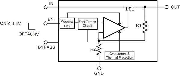
7.2 Functional Block Diagram

7.3 Feature Description
7.3.1 No-Load Stability
The LP3985 will remain stable and in regulation with no external load. This is specially important in CMOS RAM keep-alive applications.
7.3.2 On/Off Input Operation
The LP3985 is turned off by pulling the EN pin low, and turned on by pulling it high. If this feature is not used, the EN pin should be tied to VIN to keep the regulator output on at all time. To assure proper operation, the signal source used to drive the EN input must be able to swing above and below the specified turnon/turnoff voltage thresholds listed in Electrical Characteristics under VIL and VIH.
7.3.3 Fast On-Time
The LP3985 output is turned on after VREF voltage reaches its final value (1.23 V, nominal). To speed up this process, the noise reduction capacitor at the BYPASS pin is charged with an internal 70-µA current source. The current source is turned off when the bandgap voltage reaches approximately 95% of its final value. The turnon time is determined by the time constant of the bypass capacitor. The smaller the capacitor value, the shorter the turn on time, but less noise gets reduced. As a result, turn on time and noise reduction need to be taken into design consideration when choosing the value of the bypass capacitor.
7.4 Device Functional Modes
7.4.1 Operation with VOUT(TARGET) + 0.3 V ≤ VIN ≤ 6 V
The device operates if the input voltage is equal to, or exceeds, VOUT(TARGET) + 0.3 V. At input voltages below the minimum VIN requirement, the devices does not operate correctly, and output voltage may not reach target value.
7.4.2 Operation Using the EN Pin
If the voltage on the EN pin is less than 0.4 V, the device is disabled, and in this state shutdown current does not exceed 1.5 μA. Raising VEN above 1.4 V initiates the start-up sequence of the device.