SNVS087AE October   2000  – May 2015 LP3985

PRODUCTION DATA.  

  1. Features
  2. Applications
  3. Description
  4. Revision History
  5. Pin Configuration and Functions
  6. Specifications
    1. 6.1 Absolute Maximum Ratings
    2. 6.2 ESD Ratings
    3. 6.3 Recommended Operating Conditions
    4. 6.4 Thermal Information
    5. 6.5 Electrical Characteristics
    6. 6.6 Typical Performance Characteristics
  7. Detailed Description
    1. 7.1 Overview
    2. 7.2 Functional Block Diagram
    3. 7.3 Feature Description
      1. 7.3.1 No-Load Stability
      2. 7.3.2 On/Off Input Operation
      3. 7.3.3 Fast On-Time
    4. 7.4 Device Functional Modes
      1. 7.4.1 Operation with VOUT(TARGET) + 0.3 V ≤ VIN ≤ 6 V
      2. 7.4.2 Operation Using the EN Pin
  8. Application and Implementation
    1. 8.1 Application Information
    2. 8.2 Typical Application
      1. 8.2.1 Design Requirements
      2. 8.2.2 Detailed Design Procedure
        1. 8.2.2.1 External Capacitors
        2. 8.2.2.2 Input Capacitor
        3. 8.2.2.3 Output Capacitor
        4. 8.2.2.4 Capacitor Characteristics
        5. 8.2.2.5 Noise Bypass Capacitor
        6. 8.2.2.6 Thermal Considerations
      3. 8.2.3 Application Curves
  9. Power Supply Recommendations
  10. 10Layout
    1. 10.1 Layout Guidelines
    2. 10.2 Layout Examples
    3. 10.3 DSBGA Mounting
    4. 10.4 DSBGA Light Sensitivity
  11. 11Device and Documentation Support
    1. 11.1 Documentation Support
      1. 11.1.1 Related Documentation
    2. 11.2 Trademarks
    3. 11.3 Electrostatic Discharge Caution
    4. 11.4 Glossary
  12. 12Mechanical, Packaging, and Orderable Information

封装选项

机械数据 (封装 | 引脚)
散热焊盘机械数据 (封装 | 引脚)
订购信息

5 Pin Configuration and Functions

DBV Package
5 Pin SOT-23
Top View
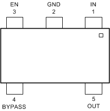
LP3985 10136407.gif
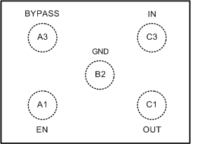
YZR Package
5 Pin DSBGA
Top View
LP3985 10136470.gif

Pin Functions

PIN TYPE DESCRIPTION
NAME DSBGA NUMBER(1) SOT-23 NUMBER
BYPASS A3 4 I/O Optional bypass capacitor for noise reduction
EN A1 3 I Enable input logic, enable high
GND B2 2 GND Common ground
IN C3 1 I Input voltage of the LDO
OUT C1 5 O Output voltage of the LDO
(1) The pin numbering scheme for the DSBGA package was revised in April 2002 to conform to JEDEC standard. Only the pin numbers were revised. No changes to the physical location of the inputs/outputs were made. For reference purposes, the obsolete numbering scheme had VEN as pin 1, GND as pin 2, VOUT as pin 3, VIN as pin 4, and BYPASS as pin 5.