SNVS161E October 2001 – October 2015 LP3988
PRODUCTION DATA.
- 1 Features
- 2 Applications
- 3 Description
- 4 Revision History
- 5 Pin Configuration and Functions
- 6 Specifications
- 7 Parameter Measurement Information
- 8 Detailed Description
- 9 Application and Implementation
- 10Power Supply Recommendations
- 11Layout
- 12Device and Documentation Support
- 13Mechanical, Packaging, and Orderable Information
1 Features
- Input Voltage Range: 2.5 V to 6 V
- Output Current: 150 mA
- PSRR at 10 kHz: 40 dB
- Quiescent Current When Shut Down: ≤ 1µA
- Fast Turnon Time: 100 µs (Typical)
- Dropout With 150-mA load: 80 mV (Typical)
- Junction Temperature Range for Operation: −40°C to +125°C
- Power-Good Flag Output
- Logic Controlled Enable
- Thermal Shutdown and Short-Circuit Current Limit
- Stable with Ceramic and High-Quality Tantalum Capacitors
2 Applications
- CDMA Cellular Handsets
- Wideband CDMA Cellular Handsets
- GSM Cellular Handsets
- Portable Information Appliances
- Tiny 3.3 V ± 5% to 2.85 V, 150-mA Converter
3 Description
The LP3988 is a 150-mA low dropout regulator designed specially to meet requirements of portable battery applications. The LP3988 is designed to work with space-saving, small 1-µF ceramic capacitors. The LP3988 features a Power Good (PG) output that indicates a faulty output condition. The device is ideal for mobile phone and similar battery-powered wireless applications. It provides up to 150 mA output current from a 2.5-V to 6-V input, consuming less than 1 µA in disable mode and has fast turnon time less than 200 µs.
The LP3988 device's performance is optimized for battery-powered systems to deliver low noise, extremely low dropout voltage, and low quiescent current. Regulator ground current increases only slightly in dropout, further prolonging the battery life.
Power supply rejection is better than 60 dB at low frequencies and starts to roll off at 10 kHz. High power-supply rejection is maintained down to lower input-voltage levels common to battery-operated circuits.
The LP3988 is available in a 5-pin SOT-23 package and a 5-pin thin DSBGA package. Performance is specified for −40°C to +125°C temperature range. For all available output voltage and package options, see the Package Option Addendum (POA) at the end of the data sheet.
Device Information(1)
| PART NUMBER | PACKAGE | BODY SIZE (NOM) |
|---|---|---|
| LP3988 | SOT-23 (5) | 2.90 mm × 1.60 mm |
| DSBGA (5) | 1.502 mm × 1.045 mm(2) |
- For all available packages, see the orderable addendum at the end of the data sheet.
- Body size dimension is maximum.
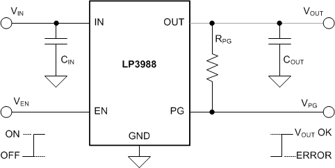
Simplified Schematic
