SNVS161E October 2001 – October 2015 LP3988
PRODUCTION DATA.
- 1 Features
- 2 Applications
- 3 Description
- 4 Revision History
- 5 Pin Configuration and Functions
- 6 Specifications
- 7 Parameter Measurement Information
- 8 Detailed Description
- 9 Application and Implementation
- 10Power Supply Recommendations
- 11Layout
- 12Device and Documentation Support
- 13Mechanical, Packaging, and Orderable Information
8 Detailed Description
8.1 Overview
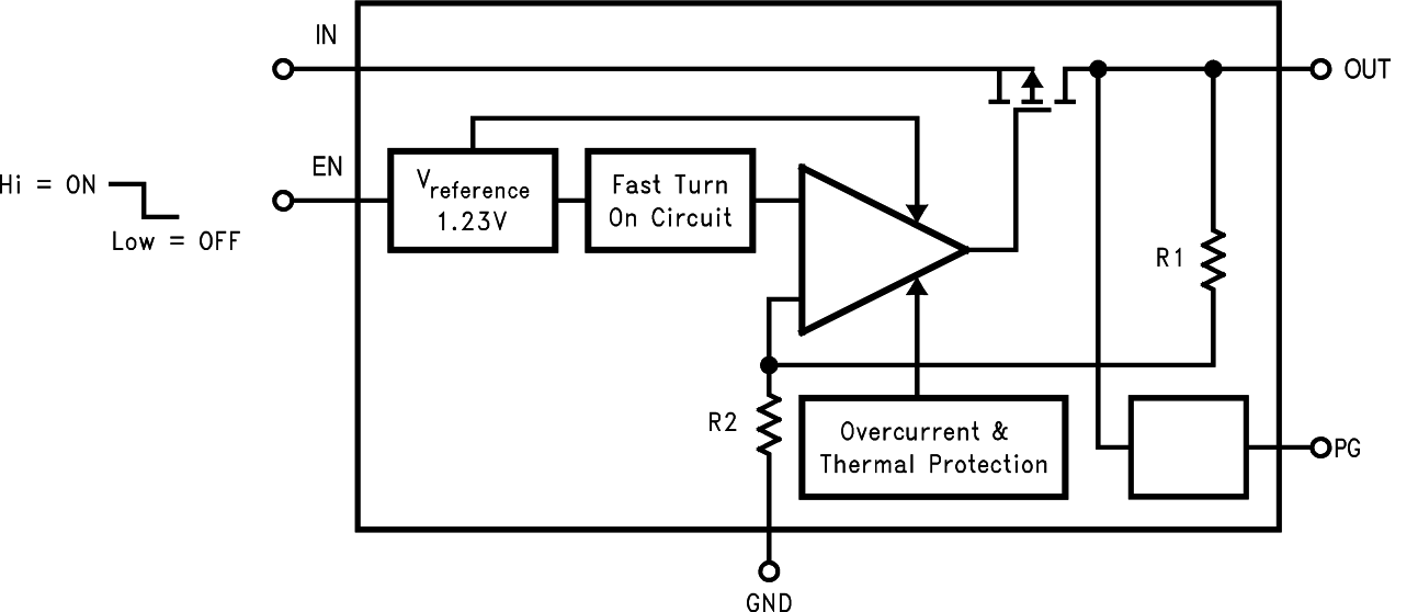
The LP3988 is a combination of a low-dropout linear regulator with an enable function, along with a Power Good (PG) output. The enable function allows the LP3988 output to be selectively enabled, or disabled, as needed. The PG output goes high when the LP3988 output voltage is typically above 95% of nominal.
8.2 Functional Block Diagram

8.3 Feature Description
8.3.1 Enable (EN)
A high input on the EN pin (VEN ≥ VIH) actives the device which turns the regulator to an ON state. A low input on the EN pin (VEN ≤ VIL) disables the device which turns the regulator to an OFF state. Operating with VEN between the VIL and the VIH thresholds is not recommended as the device status cannot be assured. For self-bias applications where the EN function is not needed, connect the EN pin to the IN pin.
8.3.2 Regulated Output (OUT)
The OUT pin is the regulated output voltage based on the internally pre-programmed voltage. The output has current limitation. In the event that the regulator drops out of regulation due to low input voltage, the output tracks the input minus a drop based on the load current. There is no UVLO circuitry. Device behavior is undefined when VIN is below the minimum operating input voltage of either 2.5 V, or VOUT + 200 mV, whichever is greater.
8.3.3 Power Good (PG) Output
The PG pin is an open-drain output and can be pulled up to any 6 V, or lower rail through an external pullup resistor. The PG pin is high-impedance when VOUT is greater than the PG trip high threshold (VTHH). If VOUT is less than the PG trip low threshold (VTHL), the open-drain output turns on and pulls the PG output low. If output voltage monitoring is not needed, the PG pin can be left floating or connected to GND. The behavior of the power-good feature is not ensured when VIN is less than 2.5 V.
8.3.4 PG Delay Time
The power-good delay times (tON, tOFF) are defined as the time period from when VOUT crosses either the PG high trip threshold voltage (VTHH), or the PG low trip threshold voltage (VTHL), to when the PG output changes to the appropriate state. The power-good delay times are set internally, and both are typically 10 µs. There is no external adjustment available to alter the delay times.
8.3.5 Current Limit
The fixed current limit (ISC) of the LP3988 helps protect the regulator during output fault conditions. The maximum amount of current the device can source is typically 600 mA, and is largely independent of input and output voltage. For reliable operation, do not operate the device in current limit for extended periods of time. Depending on power dissipation, thermal resistance, and ambient temperature, operating at the current limit may activate the thermal shutdown circuitry.
8.3.6 Thermal Shutdown (TSD)
Thermal shutdown (TSD) protection disables the output when the junction temperature rises to approximately 160°C, This shutdown causes the device dissipation to go to zero, which allows the device to cool. When the device junction temperature cools to approximately 140°C, the output circuitry is automatically enabled. Depending on power dissipation, thermal resistance, and ambient temperature, the thermal protection circuit may cycle ON and OFF. This cycling limits the dissipation of the regulator, protecting it from damage as a result of overheating. The thermal shutdown circuitry of the LP3988 has been designed to protect against temporary thermal overload conditions. The TSD circuitry was not intended to replace proper heat-sinking. Continuously running the LP3988 device in TSD may degrade device reliability and lifetime.
8.4 Device Functional Modes
8.4.1 Normal Operation
The device regulates to the nominal output voltage under the following conditions:
- The input voltage (VIN ) is at least either 2.5 V, or VOUT + 200 mV, whichever is greater.
- The enable voltage (VEN) is at least 1.2 V (VIH).
- The output current is no more than the maximum rated current of 150 mA.
- The device junction temperature (TJ) is no more than the maximum specified operating junction temperature.
8.4.2 Dropout Operation
If the input voltage is lower than the nominal output voltage plus the specified dropout voltage (VDO), but all other conditions are met for normal operation, the device operates in dropout mode. In this mode of operation, the output voltage is the same as the input voltage minus the dropout voltage. The transient performance of the device is significantly degraded because the pass device (PMOS transistor), no longer controls the current through the LDO. Line or load transients while operating in dropout can result in large output voltage deviations.
8.4.3 Disabled
The device is disabled under the following conditions:
- VEN is no more than 0.6 V (VIL).
- TJ is greater than the thermal shutdown temperature.