SNVS161E October 2001 – October 2015 LP3988
PRODUCTION DATA.
- 1 Features
- 2 Applications
- 3 Description
- 4 Revision History
- 5 Pin Configuration and Functions
- 6 Specifications
- 7 Parameter Measurement Information
- 8 Detailed Description
- 9 Application and Implementation
- 10Power Supply Recommendations
- 11Layout
- 12Device and Documentation Support
- 13Mechanical, Packaging, and Orderable Information
11 Layout
11.1 Layout Guidelines
The dynamic performance of the LP3988 is dependant on the layout of the PCB. PCB layout practices that are adequate for typical LDOs may degrade the PSRR, noise, or transient performance of the LP3988.
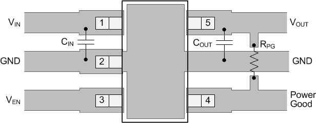
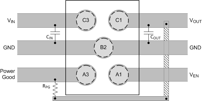
Best performance is achieved by placing CIN and COUT on the same side of the PCB as the LP3988 device, and as close as is practical to the package. The ground connections for CIN and COUT must be back to the LP3988 GND pin using as wide and as short of a copper trace as is practical.
Avoid connections using long trace lengths, narrow trace widths, and/or connections through vias. These add parasitic inductances and resistance that results in inferior performance especially during transient conditions.
The PG pin pullup resistor should be connected to the LP3988 OUT pin, with the pullup resistor located as close to the PG pin as is practical.
11.2 Layout Examples
 Figure 17. LP3988 SOT-23 Layout Example
 Figure 18. LP3988 DSBGA Layout Example
11.3 DSBGA Mounting
The DSBGA package requires specific mounting techniques, which are detailed in TI Application Note AN-1112 DSBGA Wafer Level Chip Scale Package (SNVA009). For best results during assembly, alignment ordinals on the PC board may be used to facilitate placement of the DSBGA device.