SNVS161E October   2001  – October 2015 LP3988

PRODUCTION DATA.  

  1. Features
  2. Applications
  3. Description
  4. Revision History
  5. Pin Configuration and Functions
  6. Specifications
    1. 6.1 Absolute Maximum Ratings
    2. 6.2 ESD Ratings
    3. 6.3 Recommended Operating Conditions
    4. 6.4 Thermal Information
    5. 6.5 Electrical Characteristics
    6. 6.6 Timing Requirements
    7. 6.7 Typical Characteristics
  7. Parameter Measurement Information
  8. Detailed Description
    1. 8.1 Overview
    2. 8.2 Functional Block Diagram
    3. 8.3 Feature Description
      1. 8.3.1 Enable (EN)
      2. 8.3.2 Regulated Output (OUT)
      3. 8.3.3 Power Good (PG) Output
      4. 8.3.4 PG Delay Time
      5. 8.3.5 Current Limit
      6. 8.3.6 Thermal Shutdown (TSD)
      7. 8.3.7 Fast Turnon Time
    4. 8.4 Device Functional Modes
      1. 8.4.1 Normal Operation
      2. 8.4.2 Dropout Operation
      3. 8.4.3 Disabled
  9. Application and Implementation
    1. 9.1 Application Information
    2. 9.2 Typical Application
      1. 9.2.1 Design Requirements
      2. 9.2.2 Detailed Design Procedure
        1. 9.2.2.1 External Capacitors
        2. 9.2.2.2 Input Capacitor
        3. 9.2.2.3 Output Capacitors
        4. 9.2.2.4 No-Load Stability
        5. 9.2.2.5 Capacitor Characteristics
        6. 9.2.2.6 Power Dissipation
        7. 9.2.2.7 Estimating Junction Temperature
      3. 9.2.3 Application Curves
  10. 10Power Supply Recommendations
  11. 11Layout
    1. 11.1 Layout Guidelines
    2. 11.2 Layout Examples
    3. 11.3 DSBGA Mounting
  12. 12Device and Documentation Support
    1. 12.1 Related Documentation
    2. 12.2 Community Resources
    3. 12.3 Trademarks
    4. 12.4 Electrostatic Discharge Caution
    5. 12.5 Glossary
  13. 13Mechanical, Packaging, and Orderable Information

封装选项

机械数据 (封装 | 引脚)
散热焊盘机械数据 (封装 | 引脚)
订购信息

5 Pin Configuration and Functions

DBV Package
5-Pin SOT-23
Top View
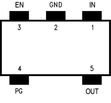
LP3988 20020507.png
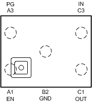
YZR Package
5-Pin DSBGA
Top View
LP3988 20020530.gif

Pin Functions

PIN TYPE DESCRIPTION
NAME DSBGA SOT-23
EN A1 3 Input Enable input logic, enable high
GND B2 2 Ground Common ground
IN C3 1 Input Input voltage of the LDO
PG A3 4 Output Power Good flag (output): open-drain output, connected to an external pullup resistor. Active low indicates an output voltage out of tolerance condition.
OUT C1 5 Output Output voltage of the LDO