SNVS161E October 2001 – October 2015 LP3988
PRODUCTION DATA.
- 1 Features
- 2 Applications
- 3 Description
- 4 Revision History
- 5 Pin Configuration and Functions
- 6 Specifications
- 7 Parameter Measurement Information
- 8 Detailed Description
- 9 Application and Implementation
- 10Power Supply Recommendations
- 11Layout
- 12Device and Documentation Support
- 13Mechanical, Packaging, and Orderable Information
6 Specifications
6.1 Absolute Maximum Ratings
over operating free-air temperature range (unless otherwise noted)(1)(2)(3)| MIN | MAX | UNIT | ||
|---|---|---|---|---|
| IN pin | −0.3 | 6.5 | V | |
| OUT, EN, PG pins | −0.3 | See(4) | V | |
| Junction temperature, TJ | 150 | °C | ||
| Power dissipation(5) | SOT-23-5 | 469 | mW | |
| DSBGA | 441 | |||
| Storage temperature, Tstg | −65 | 150 | °C | |
(1) Stresses beyond those listed under Absolute Maximum Ratings may cause permanent damage to the device. These are stress ratings only, which do not imply functional operation of the device at these or any other conditions beyond those indicated under Recommended Operating Conditions. Exposure to absolute-maximum-rated conditions for extended periods may affect device reliability.
(2) All voltages are with respect to the potential at the GND pin.
(3) If Military/Aerospace specified devices are required, contact the Texas Instruments Sales Office/ Distributors for availability and specifications.
(4) The lesser of VIN + 0.3 V or 6 V.
(5) The absolute maximum power dissipation depends on the ambient temperature and the RθJA value; it can be calculated using the formula: PD = (TJ – TA)/RθJA where TJ(MAX) is the maximum junction temperature, TA(MAX) is the maximum expected ambient temperature, and RθJA is the junction-to-ambient thermal resistance.The 469-mW rating for the SOT-23-5 package results from substituting the junction temperature, 150°C, for TJ(MAX), 70°C for TA, and 181.2°C/W for RθJA. More power can be dissipated safely at ambient temperatures below 70°C . Less power can be dissipated safely at ambient temperatures above 70°C. The absolute maximum power dissipation can be increased by 5.86 mW for each degree below 70°C, and it must be derated by 5.86 mW for each degree above 70°C. Same principle applies to the DSBGA package.
6.2 ESD Ratings
| VALUE | UNIT | |||
|---|---|---|---|---|
| LP3988 IN SOT-23 PACKAGE | ||||
| V(ESD) | Electrostatic discharge | Human-body model (HBM), per ANSI/ESDA/JEDEC JS-001(1) | ±2000 | V |
| Charged-device model (CDM), per JEDEC specification JESD22-C101(2) | ±150 | |||
| LP3988 IN DSBGA PACKAGE | ||||
| V(ESD) | Electrostatic discharge | Human-body model (HBM), per ANSI/ESDA/JEDEC JS-001(1) | ±2000 | V |
| Charged-device model (CDM), per JEDEC specification JESD22-C101(2) | ±200 | |||
(1) JEDEC document JEP155 states that 500-V HBM allows safe manufacturing with a standard ESD control process.
(2) JEDEC document JEP157 states that 250-V CDM allows safe manufacturing with a standard ESD control process.
6.3 Recommended Operating Conditions
over operating free-air temperature range (unless otherwise noted)(1)(2)| MIN | NOM | MAX | UNIT | ||
|---|---|---|---|---|---|
| VIN | 2.5(3) | 6 | V | ||
| VOUT, VEN | 0 | VIN | V | ||
| VPG | 0 | 6 | V | ||
| IPG | 0 | 500 | µA | ||
| Junction temperature, TJ | –40 | 125 | °C | ||
| Maximum power dissipation(4) | SOT-23 | 322 | mW | ||
| DSBGA | 303 | ||||
(1) Stresses beyond those listed under Absolute Maximum Ratings may cause permanent damage to the device. These are stress ratings only, which do not imply functional operation of the device at these or any other conditions beyond those indicated under Recommended Operating Conditions. Exposure to absolute-maximum-rated conditions for extended periods may affect device reliability.
(2) All voltages are with respect to the potential at the GND pin.
(3) The minimum VIN is dependant on the device output option. For VOUT(NOM) < 2.5 V, VIN(MIN) equals 2.5 V. For VOUT(NOM) ≥ 2.5 V, VIN(MIN) equals VOUT(NOM) + 200 mV.
(4) Like the Absolute Maximum power dissipation, the maximum power dissipation for operation depends on the ambient temperature. The 322-mW rating appearing under Recommended Operating Conditions for the SOT-23-5 package results from substituting the maximum junction temperature for operation, 125°C, for TJ(MAX), 70°C for TA(MAX), and 181.2°C/W for RθJA. More power can be dissipated at ambient temperatures below 70°C . Less power can be dissipated at ambient temperatures above 70°C. The maximum power dissipation for operation can be increased by 4.5 mW for each degree below 70°C, and it must be derated by 5.86 mW for each degree above 70°C. The same principle applies to the DSBGA package.
6.4 Thermal Information
| THERMAL METRIC(1) | LP3988 | UNIT | ||
|---|---|---|---|---|
| DBV (SOT-23) | YZR (DSBGA) | |||
| 5 PINS | 5 PINS | |||
| RθJA | Junction-to-ambient thermal resistance | 170.5 | 181.2 | °C/W |
| RθJC(top) | Junction-to-case (top) thermal resistance | 124.4 | 0.8 | °C/W |
| RθJB | Junction-to-board thermal resistance | 30.9 | 107.9 | °C/W |
| ψJT | Junction-to-top characterization parameter | 17.6 | 0.5 | °C/W |
| ψJB | Junction-to-board characterization parameter | 30.4 | 107.9 | °C/W |
| RθJC(bot) | Junction-to-case (bottom) thermal resistance | n/a | n/a | °C/W |
(1) For more information about traditional and new thermal metrics, see the Semiconductor and IC Package Thermal Metrics application report, SPRA953.
6.5 Electrical Characteristics
Unless otherwise specified: VEN = 1.8 V, VIN = VOUT + 0.5 V, CIN = 1 µF, IOUT = 1 mA, COUT = 1 µF; typical values and limits are for TJ = 25°C, and minimum and maximum values and limits apply over the entire junction temperature range for operation, −40°C to +125°C.(1)(2)| PARAMETER | TEST CONDITIONS | MIN | TYP | MAX | UNIT | |
|---|---|---|---|---|---|---|
| ΔVOUT | Output voltage volerance | −2 | 2 | % of VOUT(NOM) | ||
| −20°C ≤ TJ ≤ 125°C, SOT-23-5 | –3 | 3 | ||||
| SOT-23-5 | –3.5 | 3.5 | ||||
| DSBGA | –3 | 3 | ||||
| Line regulation error | VIN = VOUT(NOM) + 0.5 V to 6 V TJ = 25°C |
−0.15 | 0.15 | %/V | ||
| VIN = VOUT(NOM) + 0.5 V to 6 V | –0.2 | 0.2 | ||||
| Load regulation error(3) | IOUT = 1 mA to 150 mA, TJ = 25°C | 0.005 | %/mA | |||
| IOUT = 1 mA to 150 mA | 0.007 | |||||
| PSRR | Power Supply Rejection Ratio | VIN = VOUT(NOM) + 1 V, ƒ = 1 kHz, IOUT = 50 mA (See Figure 11) |
65 | dB | ||
| VIN = VOUT(nom) + 1 V, ƒ = 10 kHz, IOUT = 50 mA (See Figure 11) |
45 | |||||
| IQ | Quiescent current | VEN = 1.4 V, IOUT = 0 mA, TJ = 25°C | 85 | 120 | µA | |
| VEN = 1.4 V, IOUT = 0 to 150 mA | 140 | 200 | ||||
| VEN = 0.4 V | 0.003 | 1 | ||||
| Dropout voltage(4) | IOUT = 1 mA | 1 | 5 | mV | ||
| IOUT = 150 mA, TJ = 25°C | 80 | 115 | ||||
| IOUT = 150 mA | 150 | |||||
| ISC | Short circuit current limit | See(5) | 600 | mA | ||
| en | Output noise voltage | BW = 10 Hz to 100 kHz, COUT = 1 µF |
220 | µVRMS | ||
| COUT | Output capacitor | Capacitance(6) | 1 | 20 | µF | |
| ESR(6) | 5 | 500 | mΩ | |||
| TSD | Thermal shutdown temperature | 160 | °C | |||
| Thermal shutdown hysteresis | 20 | |||||
| ENABLE CONTROL CHARACTERISTICS | ||||||
| IEN | Maximum input current at EN | VEN = 0 V and VIN = 6 V | 0.1 | µA | ||
| VIL | Logic low input threshold | VIN = 2.5 V to 6 V | 0.5 | V | ||
| VIH | Logic high input threshold | VIN = 2.5 V to 6 V | 1.2 | V | ||
| POWER GOOD | ||||||
| VTHL | PG low threshold (See Figure 10) |
% of VOUT (PG ON), TJ = 25°C | 90% | 93% | 95% | |
| VTHH | PG high threshold (See Figure 10) |
% of VOUT (PG OFF), TJ = 25°C(7) | 92% | 95% | 98% | |
| VOL | PG output logic low voltage | IPULLUP = 100 µA, fault condition | 0.02 | 0.1 | V | |
| IPGL | PG output leakage current | PG off, VPG = 6 V | 0.02 | µA | ||
(1) All electrical characteristics having room-temperature limits are tested during production with TJ = 25°C or correlated using Statistical Quality Control (SQC) methods. All hot and cold limits are specified by correlating the electrical characteristics to process and temperature variations and applying statistical process control.
(2) The target output voltage, which is labeled VOUT(NOM), is the desired voltage option.
(3) An increase in the load current results in a slight decrease in the output voltage and vice versa.
(4) Dropout voltage is the input-to-output voltage difference at which the output voltage is 100 mV below its nominal value.
(5) Short-circuit current is measured on input supply line after pulling down VOUT to 95% VOUT(NOM).
(6) Specified by design. Not production tested. The capacitor tolerance should be ±30% or better over the full temperature range. The full range of operating conditions such as temperature, DC bias and even capacitor case size for the capacitor in the application should be considered during device selection to ensure this minimum capacitance specification is met. X7R capacitor types are recommended to meet the full device temperature range.
(7) The low and high thresholds are generated together. Typically a 2.6% difference is seen between these thresholds.
6.6 Timing Requirements
| MIN | NOM | MAX | UNIT | ||
|---|---|---|---|---|---|
| TON | PG turnon time(1), VIN = 4.2 V | 10 | µs | ||
| TOFF | PG turnoff time(1), VIN = 4.2 V | 10 | µs | ||
(1) Turnon time is time measured between the enable input just exceeding VIH and the output voltage just reaching 95% of its nominal value.
6.7 Typical Characteristics
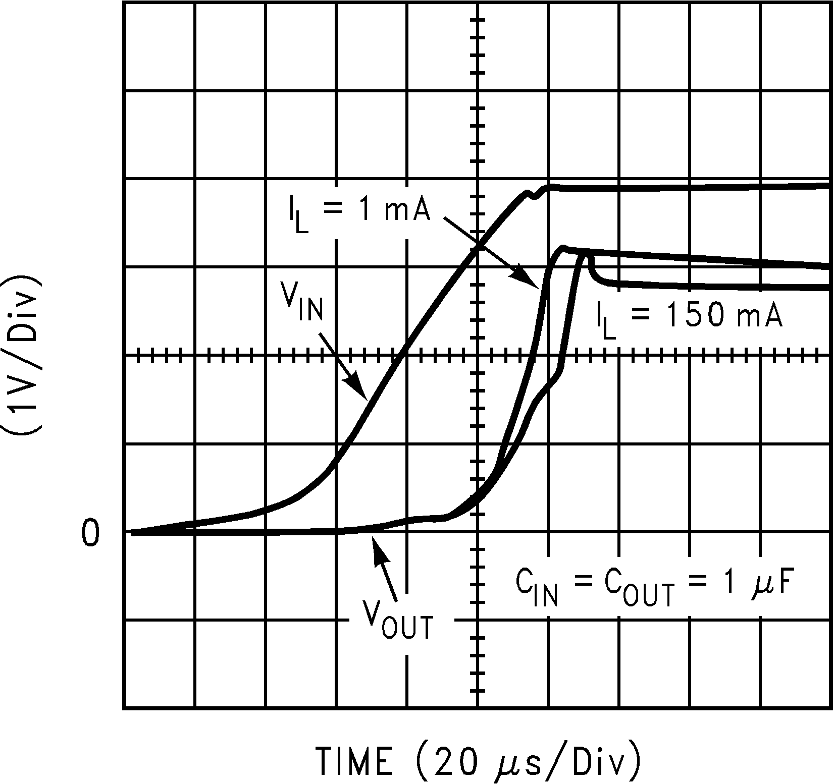
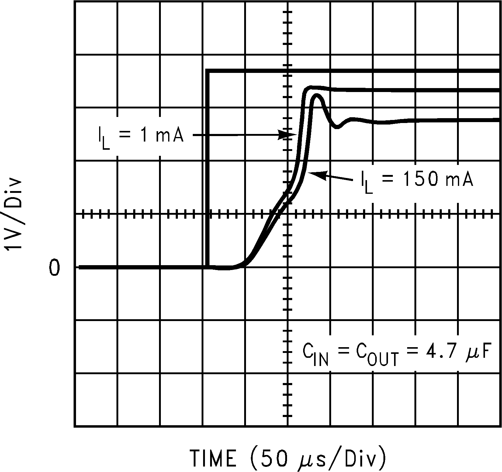
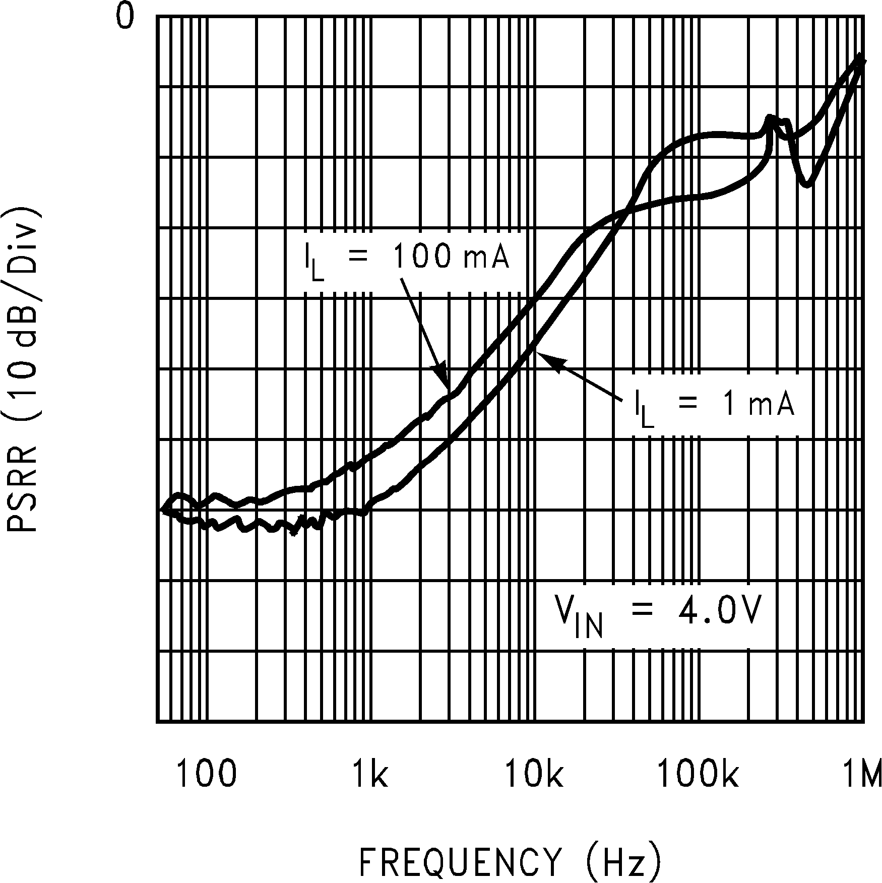
Unless otherwise specified, CIN = COUT = 1 µF ceramic, VIN = VOUT + 0.2 V, TA = 25°C, EN pin is tied to VIN.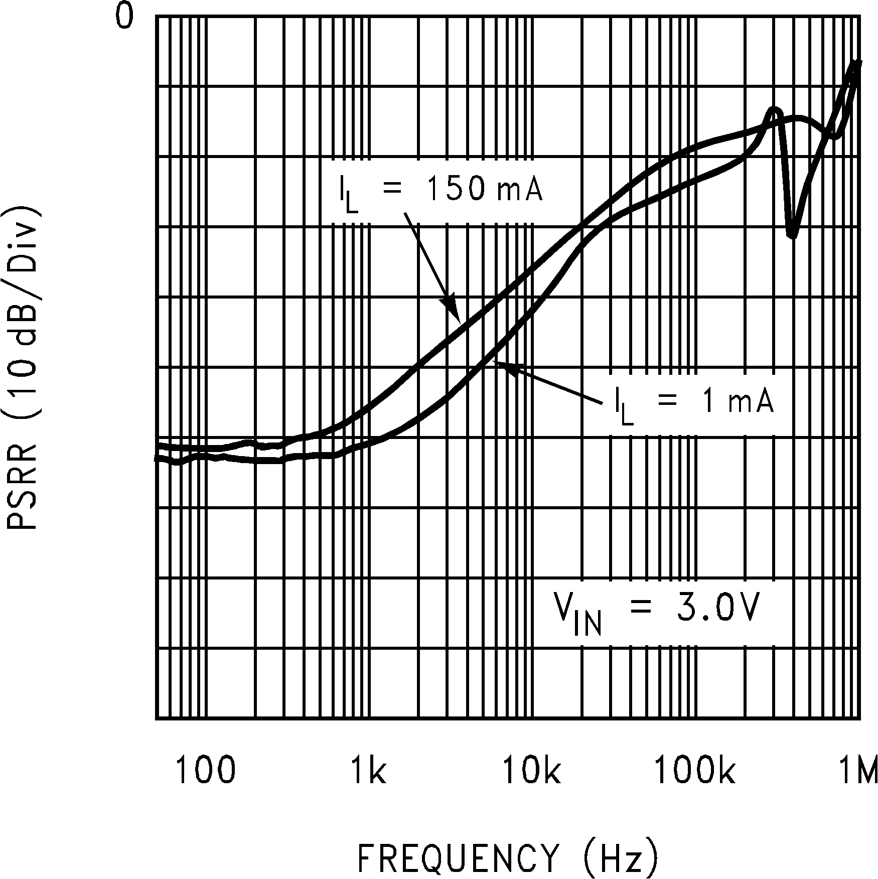
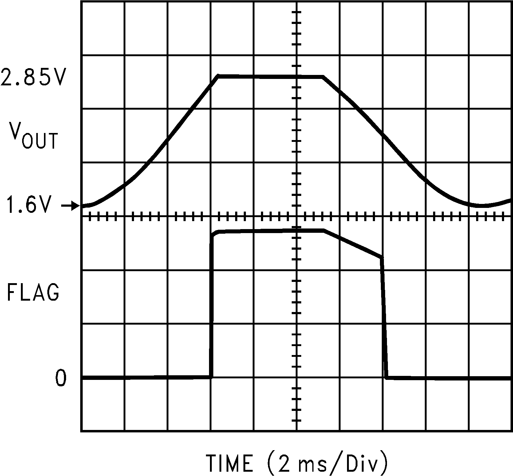
(Flag Pin Pulled To VOUT Through a 100-kΩ Resistor)
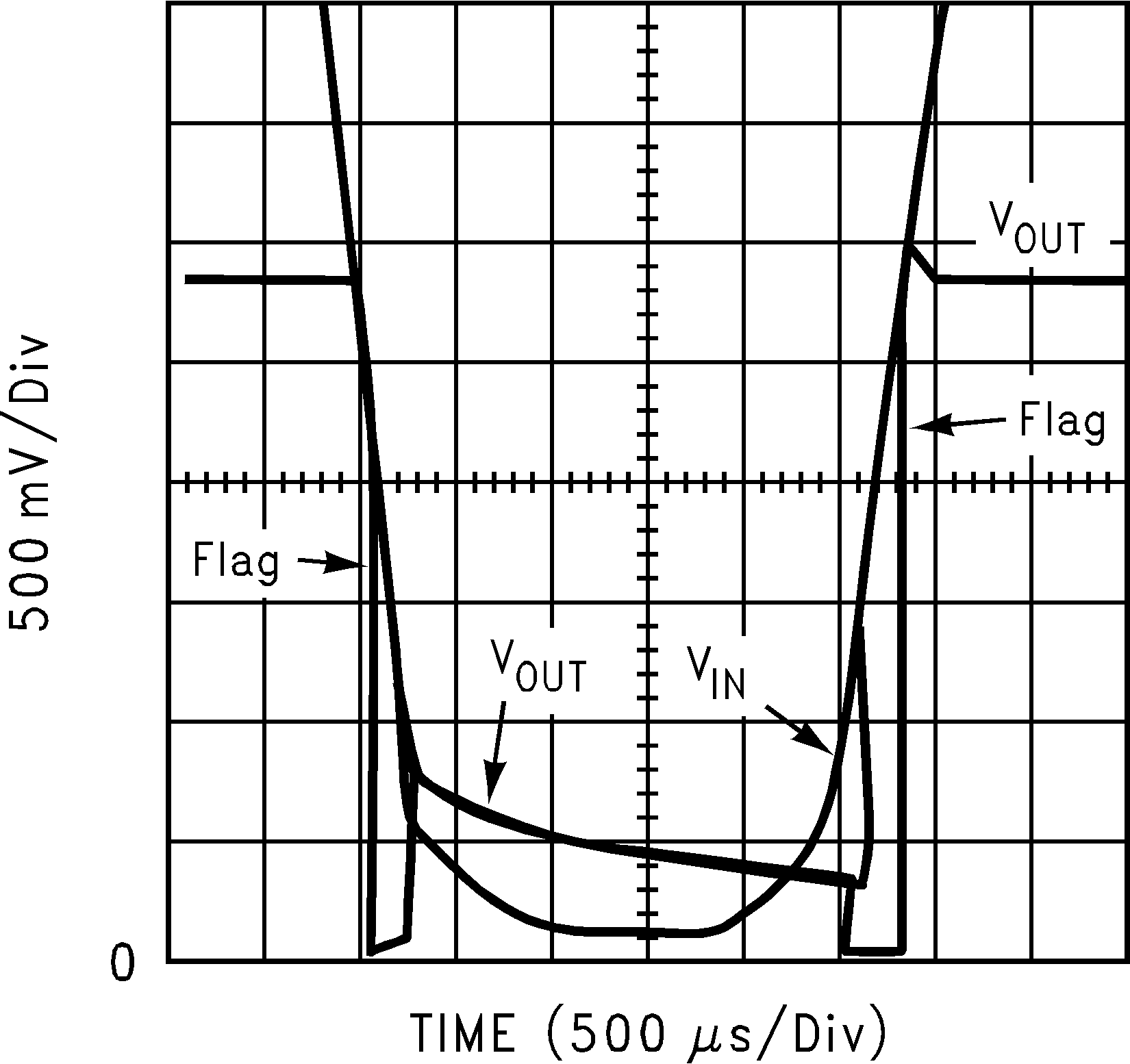
(Flag Pin Pulled To VOUT Through a 100-kΩ Resistor)
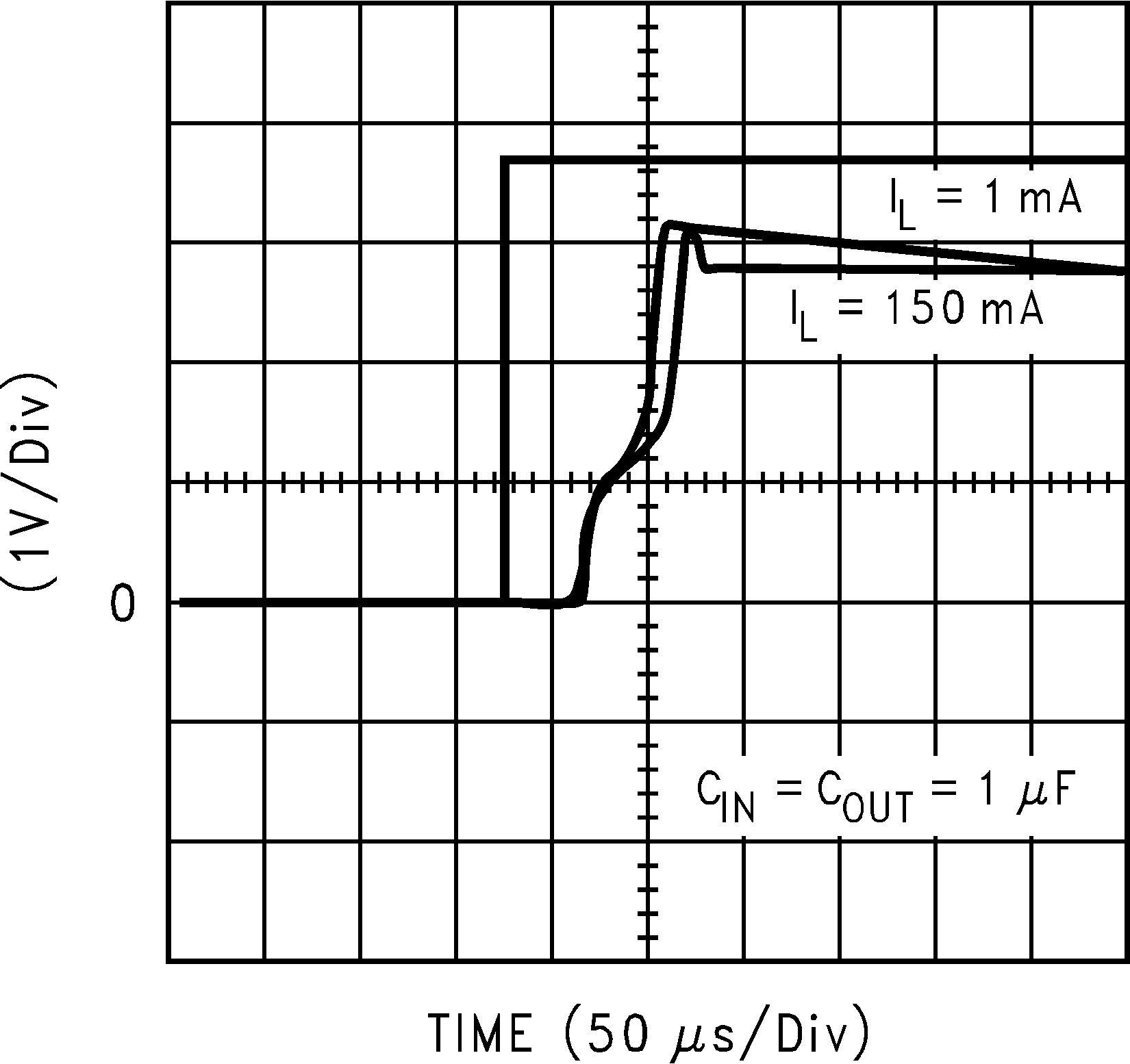
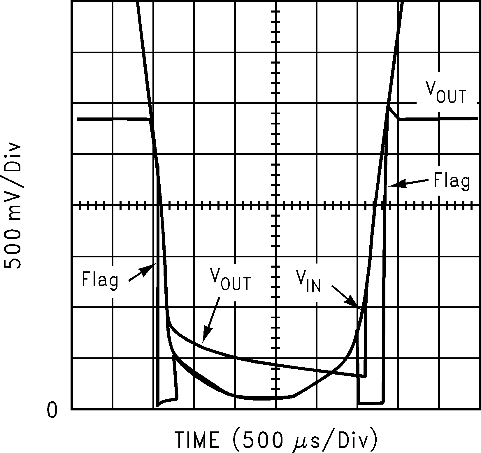
(Flag Pin Pulled To VIN Through a 100-kΩ Resistor)
