LP3990 150-mA Linear Voltage Regulator for Digital Applications
1 Features
- 1% Voltage Accuracy at Room Temperature
- Stable with Ceramic Capacitor
- Logic Controlled Enable
- No Noise Bypass Capacitor Required
- Thermal-Overload and Short-Circuit Protection
- Input Voltage Range, 2 V to 6 V
- Output Voltage Range, 0.8 V to 3.3 V
- Output Current, 150 mA
- Output Stable - Capacitors, 1 µF
- Virtually Zero IQ (Disabled), < 10 nA
- Very Low IQ (Enabled), 43 µA
- Low Output Noise, 150 µVRMS
- PSRR, 55 dB at 1 kHz
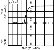
- Fast Start-Up, 105 µs
2 Applications
- Cellular Handsets
- Hand-Held Information Appliances
3 Description
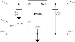
The LP3990 regulator is designed to meet the requirements of portable, battery-powered systems providing an accurate output voltage, low-noise, and low-quiescent current. The LP3990 will provide a 0.8-V output from the low input voltage of 2 V at up to a 150-mA load current. When switched into shutdown mode via a logic signal at the enable pin (EN), the power consumption is reduced to virtually zero.
The LP3990 is designed to be stable with space-saving ceramic capacitors with values as low as 1 µF.
Performance is specified for a –40°C to 125°C junction temperature range.
For output voltages other than 0.8 V, 1.2 V, 1.35 V, 1.5 V, 1.8 V, 2.5 V, 2.8 V, or 3.3 V, please contact the Texas Instruments sales office.
Device Information(1)
| PART NUMBER | PACKAGE | BODY SIZE (NOM) |
|---|---|---|
| LP3990 | DSBGA (4) | 1.324 mm x 1.045 mm (MAX) |
| WSON (6) | 2.90 mm x 1.60 mm | |
| SOT-23 (5) | 3.00 mm x 3.00 mm |
- For all available packages, see the orderable addendum at the end of the datasheet.
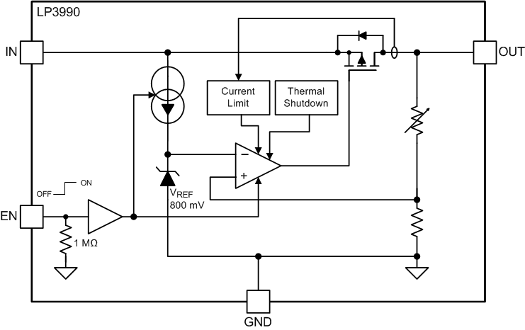
Simplified Schematic
4 Revision History
Changes from I Revision (May 2013) to J Revision
- Added Device Information and Handling Rating tables, Feature Description, Device Functional Modes, Application and Implementation, Power Supply Recommendations, Layout, Device and Documentation Support, and Mechanical, Packaging, and Orderable Information sections; moved some curves to Application Curves sectionGo
5 Pin Configuration and Functions
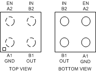
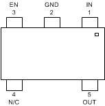
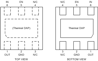
Pin Functions
| PIN | I/O | DESCRIPTION | |||
|---|---|---|---|---|---|
| NAME | DSBGA | SOT-23 | WSON | ||
| YZR | DBV | NGG | |||
| GND | A1 | 2 | 2 | — | Common Ground. |
| EN | A2 | 3 | 5 | I | Enable Input; Enables the Regulator when ≥ 0.95 V. Disables the Regulator when ≤ 0.4 V. Enable Input has 1-MΩ (typical) pull-down resistor to GND. |
| OUT | B1 | 5 | 1 | O | Voltage output. A 1-µF Low ESR Capacitor should be connected to this Pin. Connect this output to the load circuit. |
| IN | B2 | 1 | 6 | I | Voltage supply Input. A 1-µF capacitor should be connected at this input. |
| N/A | 4 | 3 | I | No internal connection. | |
| N/C | N/A | 4 | I | No internal connection. | |
| N/C | Pad | — | Thermal pad. Connect to Pin 2. | ||
6 Specifications
6.1 Absolute Maximum Ratings(1)(2)(3)
over operating free-air temperature range (unless otherwise noted)| MIN | MAX | UNIT | ||
|---|---|---|---|---|
| Input voltage | –0.3 | 6.5 | V | |
| Output voltage | –0.3 | Note(4) | ||
| ENABLE input voltage | –0.3 | 6.5 | ||
| Continuous power dissipation internally limited | Note(5) | |||
6.2 Handling Ratings
| MIN | MAX | UNIT | |||
|---|---|---|---|---|---|
| Tstg | Storage temperature range | –65 | 150 | °C | |
| V(ESD) | Electrostatic discharge | Human body model (HBM), per ANSI/ESDA/JEDEC JS-001, all pins(1) | –2000 | 2000 | V |
| Charged device model (CDM), per JEDEC specification JESD22-C101, all pins | 250 | 1500 | |||
| Machine model | –200 | 200 | |||
6.3 Recommended Operating Conditions
over operating free-air temperature range (unless otherwise noted)| MIN | NOM | MAX | UNIT | ||
|---|---|---|---|---|---|
| Input voltage, VIN | 2 | 6 | V | ||
| Enable input voltage, VEN | 0.0 | VIN | |||
| Junction temperature, TJ(1) | –40 | 125 | °C | ||
6.4 Thermal Information
| THERMAL METRIC(1) | LP3990 | UNIT | |||
|---|---|---|---|---|---|
| YZR (DSBGA) | DBV (SOT-23) | NGG (WSON) | |||
| 4 PINS | 5 PINS | 6 PINS | |||
| RθJA | Junction-to-ambient thermal resistance | 188.9 | 165.2 | 53.9 | °C/W |
| RθJC(top) | Junction-to-case (top) thermal resistance | 1.0 | 69.9 | 51.2 | |
| RθJB | Junction-to-board thermal resistance | 105.3 | 27.3 | 28.2 | |
| ψJT | Junction-to-top characterization parameter | 0.7 | 1.8 | 0.6 | |
| ψJB | Junction-to-board characterization parameter | 105.2 | 26.8 | 28.3 | |
| RθJC(bot) | Junction-to-case (bottom) thermal resistance | N/A | N/A | 8.1 | |
6.5 Electrical Characteristics(1)(3)
Unless otherwise noted, VEN = 950 mV, VIN = VOUT + 1 V or VIN = 2 V, whichever is higher. CIN = 1 µF, IOUT = 1 mA, COUT = 0.47 µF.| PARAMETER | TEST CONDITIONS | MIN | TYP | MAX | UNIT | ||
|---|---|---|---|---|---|---|---|
| VIN | Input voltage | Note (2), TJ = 25°C | 2 | 6 | V | ||
| ΔVOUT | Output voltage tolerance | ILOAD = 1 mA TJ = 25°C |
DSBGA | –1 | 1% | ||
| WQFN | –1.5% | 1.5% | |||||
| SOT-23 | –1.5% | 1.5% | |||||
| Over full line and load regulation | DSBGA | –2.5% | 2.5% | ||||
| WQFN | –3% | 3% | |||||
| SOT-23 | –4% | 4% | |||||
| Line regulation error | VIN = (VOUT(NOM) + 1 V) to 6 V | 0.1 | 0.02 | 0.1 | %/V | ||
| Load regulation error | IOUT = 1 mA to 150 mA |
VOUT = 0.8 V to 1.95 V DSBGA |
–0.005 | 0.002 | 0.005 | %/mA | |
| VOUT = 0.8 V to 1.95 V WQFN, SOT-23 |
–0.008 | 0.003 | 0.008 | ||||
| VOUT = 2 V to 3.3 V DSBGA |
–0.002 | 0.0005 | 0.002 | ||||
| VOUT = 2 V to 3.3 V WQFN, SOT-23 |
–0.005 | 0.002 | 0.005 | ||||
| VDO | Dropout voltage | IOUT = 150 mA(4)(5) | 120 | 200 | mV | ||
| ILOAD | Load current | Note (5)(6), TJ = 25°C | 0 | µA | |||
| IQ | Quiescent current | VEN = 950 mV, IOUT = 0 mA | 43 | 80 | µA | ||
| VEN = 950 mV, IOUT = 150 mA | 65 | 120 | |||||
| VEN = 0.4 V (output disabled), TJ = 25°C | 0.002 | 0.2 | |||||
| ISC | Short circuit current limit | Note (7) | 550 | 1000 | mA | ||
| IOUT | Maximum output current | 150 | |||||
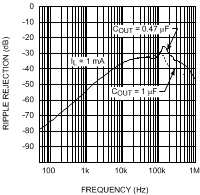
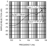
| PSRR | Power Supply Rejection Ratio | ƒ = 1 kHz, IOUT = 1 mA to 150 mA | 55 | dB | |||
| ƒ = 10 kHz, IOUT = 150 mA | 35 | ||||||
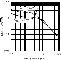
| eη | Output noise voltage(5) | BW = 10 Hz to 100 kHz | VOUT = 0.8 V | 60 | µVRMS | ||
| VOUT = 1.5 V | 125 | ||||||
| VOUT = 3.3 V | 180 | ||||||
| TSHUTDOWN | Thermal shutdown junction temperature | Junction temperature (TJ) rising until the output is disabled | 155 | °C | |||
| Hysteresis | 15 | ||||||
| ENABLE CONTROL CHARACTERISTICS | |||||||
| IEN(8) | Maximum input current at EN pin | VEN = 0 V (Output is disabled) TJ = 25°C |
0.001 | 0.1 | µA | ||
| VEN = 6 V | 2.5 | 6 | 10 | ||||
| VIL | Low input threshold | VIN = 2 V to 6 V VEN falling from ≥ VIH until the output is disabled |
0.4 | V | |||
| VIH | High input threshold | VIN = 2 V to 6 V VEN rising from ≤ VIL until the output is enabled |
0.95 | ||||
6.6 Output Capacitor, Recommended Specifications(1)
| PARAMETER | TEST CONDITIONS | MIN | TYP | MAX | UNIT | |
|---|---|---|---|---|---|---|
| COUT | Output capacitance | Capacitance(3) | 0.7(2) | 1 | 500 | µF |
| ESR | 5 | mΩ | ||||
6.7 Timing Requirements
| MIN | NOM(1) | MAX(2) | UNIT | ||||
|---|---|---|---|---|---|---|---|
| TON | Turnon time (3) | From VEN ↑ VIH to VOUT 95% level (VIN(MIN) to 6 V) |
VOUT = 0.8 V | 80 | 150 | µs | |
| VOUT = 1.5 V | 105 | 200 | |||||
| VOUT = 3.3 V | 175 | 250 | |||||
| Transient response | Line transient response (ΔVOUT) | Trise = Tfall = 30 µs(3), ΔVIN = 600 mV |
8 | 16 | mV (pk-pk) | ||
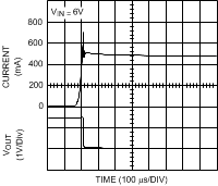
| Load transient response (ΔVOUT) | Trise = Tfall = 1 µs(3), IOUT = 1 mA to 150 mA COUT = 1 µF |
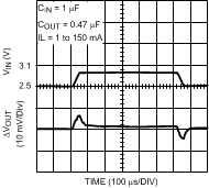
55 | 100 | mV | |||
6.8 Typical Performance Characteristics
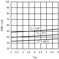
Unless otherwise specified, CIN = 1 µF ceramic, COUT = 0.47 µF ceramic, VIN = VOUT(NOM) + 1 V, TA = 25°C, VOUT(NOM) = 1.5 V; VEN = VIN.
| ILOAD = 0 mA | ||
| ILOAD = 150 mA | ||
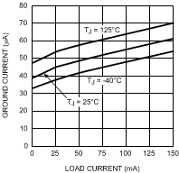
| ILOAD = 1 mA | ||
7 Detailed Description
7.1 Overview
Designed meet the requirements of portable, battery-powered digital systems providing an accurate output voltage with fast start-up. When disabled via a low logic signal at the enable pin (EN), the power consumption is reduced to virtually zero
The LP3990 is designed to perform with a single 1-μF input capacitor and a single 1-μF ceramic output capacitor.
7.2 Functional Block Diagram
7.3 Feature Description
7.3.1 Enable (EN)
The LP3990 Enable (EN) pin is internally held low by a 1-MΩ resistor to GND. The EN pin voltage must be higher than the VIH threshold to ensure that the device is fully enabled under all operating conditions. The EN pin voltage must be lower than the VIL threshold to ensure that the device is fully disabled. If the EN pin is left open the LP3990 output will be disabled.
7.3.2 Thermal Overload Protection (TSD)
Thermal Shutdown disables the output when the junction temperature rises to approximately 155°C which allows the device to cool. When the junction temperature cools to approximately 140°C, the output circuitry enables. Based on power dissipation, thermal resistance, and ambient temperature, the thermal protection circuit may cycle on and off. This thermal cycling limits the dissipation of the regulator and protects it from damage as a result of overheating.
The Thermal Shutdown circuitry of the LP3990 has been designed to protect against temporary thermal overload conditions. The Thermal Shutdown circuitry was not intended to replace proper heat-sinking. Continuously running the LP3990 device into thermal shutdown may degrade device reliability.
7.4 Device Functional Modes
7.4.1 Enable (EN)
The LP3990 EN pin is internally held low by a 1-MΩ resistor to GND. The EN pin voltage must be higher than the VIH threshold to ensure that the device is fully enabled under all operating conditions.
7.4.2 Minimum Operating Input Voltage (VIN)
The LP3990 does not include any dedicated UVLO circuitry. The LP3990 internal circuitry is not fully functional until VIN is at least 2 V. The output voltage is not regulated until VIN ≥ (VOUT + VDO), or 2 V, whichever is higher.