ZHCSJT3B May 2019 – August 2020 LP5009 , LP5012
PRODUCTION DATA
- 1 特性
- 2 应用
- 3 说明
- 4 Revision History
- 5 Description (continued)
- 6 Pin Configuration and Functions
- 7 Specifications
-
8 Detailed Description
- 8.1 Overview
- 8.2 Functional Block Diagram
- 8.3
Feature Description
- 8.3.1 PWM Control for Each Channel
- 8.3.2 LED Bank Control
- 8.3.3 Current Range Setting
- 8.3.4 Automatic Power-Save Mode
- 8.3.5 Protection Features
- 8.4 Device Functional Modes
- 8.5 Programming
- 8.6
Register Maps
- 45
- 8.6.1 DEVICE_CONFIG0 (Address = 0h) [reset = 0h]
- 8.6.2 DEVICE_CONFIG1 (Address = 1h) [reset = 3Ch]
- 8.6.3 LED_CONFIG0 (Address = 2h) [reset = 00h]
- 8.6.4 BANK_BRIGHTNESS (Address = 3h) [reset = FFh]
- 8.6.5 BANK_A_COLOR (Address = 4h) [reset = 00h]
- 8.6.6 BANK_B_COLOR (Address = 5h) [reset = 00h]
- 8.6.7 BANK_C_COLOR (Address = 6h) [reset = 00h]
- 8.6.8 LED0_BRIGHTNESS (Address = 7h) [reset = FFh]
- 8.6.9 LED1_BRIGHTNESS (Address = 8h) [reset = FFh]
- 8.6.10 LED2_BRIGHTNESS (Address = 9h) [reset = FFh]
- 8.6.11 LED3_BRIGHTNESS (Address = 0Ah) [reset = FFh]
- 8.6.12 OUT0_COLOR (Address = 0Bh) [reset = 00h]
- 8.6.13 OUT1_COLOR (Address = 0Ch) [reset = 00h]
- 8.6.14 OUT2_COLOR (Address = 0Dh) [reset = 00h]
- 8.6.15 OUT3_COLOR (Address = 0Eh) [reset = 00h]
- 8.6.16 OUT4_COLOR (Address = 0Fh) [reset = 00h]
- 8.6.17 OUT5_COLOR (Address = 10h) [reset = 00h]
- 8.6.18 OUT6_COLOR (Address = 11h) [reset = 00h]
- 8.6.19 OUT7_COLOR (Address = 12h) [reset = 00h]
- 8.6.20 OUT8_COLOR (Address = 13h) [reset = 00h]
- 8.6.21 OUT9_COLOR (Address = 14h) [reset = 00h]
- 8.6.22 OUT10_COLOR (Address = 15h) [reset = 00h]
- 8.6.23 OUT11_COLOR (Address = 16h) [reset = 00h]
- 8.6.24 RESET (Address = 17h) [reset = 00h]
- 9 Application and Implementation
- 10Power Supply Recommendations
- 11Layout
- 12Device and Documentation Support
- 13Mechanical, Packaging, and Orderable Information
封装选项
机械数据 (封装 | 引脚)
散热焊盘机械数据 (封装 | 引脚)
- RUK|20
订购信息
8.4 Device Functional Modes
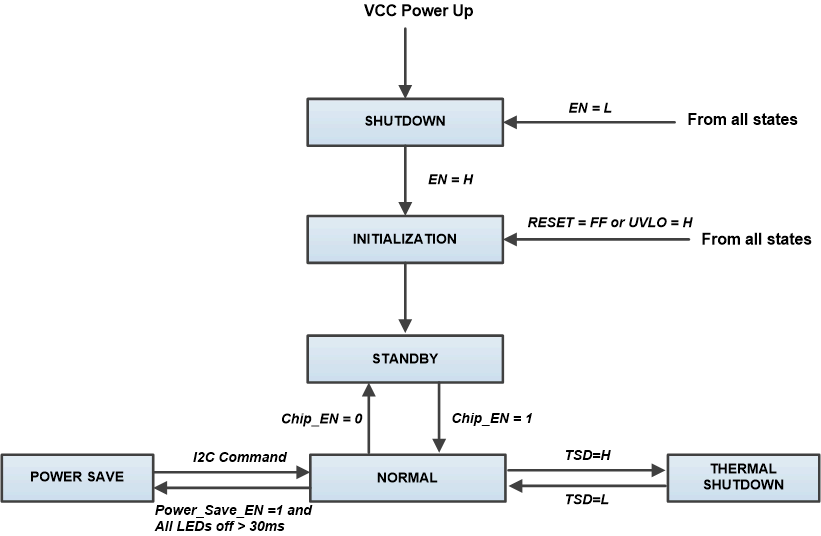
 Figure 8-7 Functional Modes
- INITIALIZATION: The device enters into INITIALIZATION mode when EN = H. In this mode, all the registers are reset. Entry can also be from any state, if the RESET (register) = FFh or UVLO is active.
- NORMAL: The device enters the NORMAL mode when Chip_EN (register) = 1. ICC is 10 mA (typical).
- POWER SAVE: The device automatically enters the POWER SAVE mode when Power_Save_EN (register) = 1 and all the LEDs are off for a duration of > 30 ms. In POWER SAVE mode, analog blocks are disabled to minimize power consumption, but the registers retain the data and keep it available via I2C. ICC is 10 µA (typical). In case of any I2C command to this device, it returns to the NORMAL mode.
- SHUTDOWN: The device enters into SHUTDOWN mode from all states on VCC power up or when EN = L. ICC is < 1 µA (maximum).
- STANDBY: The device enters the STANDBY mode when Chip_EN (register) = 0. In this mode, all the OUTx pins are shut down, but the registers retain the data and keep it available via I2C. STANDBY is the low-power-consumption mode, when all circuit functions are disabled. ICC is 10 µA (typical).
- THERMAL SHUTDOWN: The device automatically enters the THERMAL SHUTDOWN mode when the junction temperature exceeds 160°C (typical). In this mode, all the OUTx outputs are shut down. If the junction temperature decreases below 145°C (typical), the device returns to the NORMAL mode.