ZHCSHV7C October 2018 – July 2024 LP5018 , LP5024
PRODUCTION DATA
- 1
- 1 特性
- 2 应用
- 3 说明
- 4 说明(续)
- 5 Pin Configuration and Functions
- 6 Specifications
-
7 Detailed Description
- 7.1 Overview
- 7.2 Functional Block Diagram
- 7.3
Feature Description
- 7.3.1 PWM Control for Each Channel
- 7.3.2 LED Bank Control
- 7.3.3 Current Range Setting
- 7.3.4 Automatic Power-Save Mode
- 7.3.5 Protection Features
- 7.4 Device Functional Modes
- 7.5 Programming
- 7.6
Register Maps
- 7.6.1 DEVICE_CONFIG0 (Address = 0h) [reset = 0h]
- 7.6.2 DEVICE_CONFIG1 (Address = 1h) [reset = 3Ch]
- 7.6.3 LED_CONFIG0 (Address = 2h) [reset = 00h]
- 7.6.4 BANK_BRIGHTNESS (Address = 3h) [reset = FFh]
- 7.6.5 BANK_A_COLOR (Address = 4h) [reset = 00h]
- 7.6.6 BANK_B_COLOR (Address = 5h) [reset = 00h]
- 7.6.7 BANK_C_COLOR (Address = 6h) [reset = 00h]
- 7.6.8 LED0_BRIGHTNESS (Address = 7h) [reset = FFh]
- 7.6.9 LED1_BRIGHTNESS (Address = 8h) [reset = FFh]
- 7.6.10 LED2_BRIGHTNESS (Address = 9h) [reset = FFh]
- 7.6.11 LED3_BRIGHTNESS (Address = 0Ah) [reset = FFh]
- 7.6.12 LED4_BRIGHTNESS (Address = 0Bh) [reset = FFh]
- 7.6.13 LED5_BRIGHTNESS (Address = 0Ch) [reset = FFh]
- 7.6.14 LED6_BRIGHTNESS (Address = 0Dh) [reset = FFh]
- 7.6.15 LED7_BRIGHTNESS (Address = 0Eh) [reset = FFh]
- 7.6.16 OUT0_COLOR (Address = 0Fh) [reset = 00h]
- 7.6.17 OUT1_COLOR (Address = 10h) [reset = 00h]
- 7.6.18 OUT2_COLOR (Address = 11h) [reset = 00h]
- 7.6.19 OUT3_COLOR (Address = 12h) [reset = 00h]
- 7.6.20 OUT4_COLOR (Address = 13h) [reset = 00h]
- 7.6.21 OUT5_COLOR (Address = 14h) [reset = 00h]
- 7.6.22 OUT6_COLOR (Address = 15h) [reset = 00h]
- 7.6.23 OUT7_COLOR (Address = 16h) [reset = 00h]
- 7.6.24 OUT8_COLOR (Address = 17h) [reset = 00h]
- 7.6.25 OUT9_COLOR (Address = 18h) [reset = 00h]
- 7.6.26 OUT10_COLOR (Address = 19h) [reset = 00h]
- 7.6.27 OUT11_COLOR (Address = 1Ah) [reset = 00h]
- 7.6.28 OUT12_COLOR (Address = 1Bh) [reset = 00h]
- 7.6.29 OUT13_COLOR (Address = 1Ch) [reset = 00h]
- 7.6.30 OUT14_COLOR (Address = 1Dh) [reset = 00h]
- 7.6.31 OUT15_COLOR (Address = 1Eh) [reset = 00h]
- 7.6.32 OUT16_COLOR (Address = 1Fh) [reset = 00h]
- 7.6.33 OUT17_COLOR (Address = 20h) [reset = 00h]
- 7.6.34 OUT18_COLOR (Address = 21h) [reset = 00h]
- 7.6.35 OUT19_COLOR (Address = 22h) [reset = 00h]
- 7.6.36 OUT20_COLOR (Address = 23h) [reset = 00h]
- 7.6.37 OUT21_COLOR (Address = 24h) [reset = 00h]
- 7.6.38 OUT22_COLOR (Address = 25h) [reset = 00h]
- 7.6.39 OUT23_COLOR (Address = 26h) [reset = 00h]
- 7.6.40 RESET (Address = 27h) [reset = 00h]
- 8 Application and Implementation
- 9 Device and Documentation Support
- 10Revision History
- 11Mechanical, Packaging, and Orderable Information
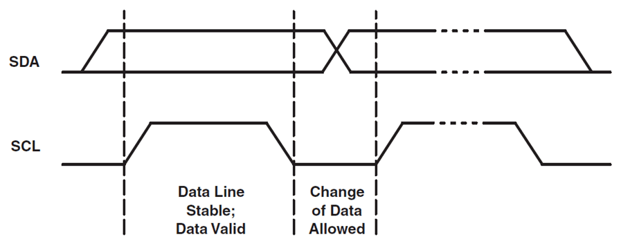
7.5.1.1 Data Validity
The data on SDA line must be stable during the HIGH period of the clock signal (SCL). In other words, the state of the data line can only be changed when the clock signal is LOW.
 Figure 7-8 Data Validity