SNVS441I January 2007 – November 2016 LP5521
PRODUCTION DATA.
- 1 Features
- 2 Applications
- 3 Description
- 4 Revision History
- 5 Pin Configuration and Functions
-
6 Specifications
- 6.1 Absolute Maximum Ratings
- 6.2 ESD Ratings
- 6.3 Recommended Operating Conditions
- 6.4 Thermal Information
- 6.5 Electrical Characteristics
- 6.6 Charge Pump Electrical Characteristics
- 6.7 LED Driver Electrical Characteristics (R, G, B Outputs)
- 6.8 Logic Interface Characteristics
- 6.9 I2C Timing Requirements (SDA, SCL)
- 6.10 Typical Characteristics
-
7 Detailed Description
- 7.1 Overview
- 7.2 Functional Block Diagram
- 7.3 Feature Description
- 7.4 Device Functional Modes
- 7.5 Programming
- 7.6
Register Maps
- 7.6.1 Enable Register (Enable)
- 7.6.2 Operation Mode Register (OP Mode)
- 7.6.3 R Channel PWM Control (R_PWM)
- 7.6.4 G Channel PWM Control (G_PWM)
- 7.6.5 B Channel PWM Control (B_PWM)
- 7.6.6 R Channel Current (R_CURRENT)
- 7.6.7 G Channel Current (G_CURRENT)
- 7.6.8 B Channel Current (B_CURRENT)
- 7.6.9 Configuration Control (CONFIG)
- 7.6.10 R Channel Program Counter Value (R Channel PC)
- 7.6.11 G Channel Program Counter Value (G Channel PC)
- 7.6.12 B Channel Program Counter Value (B Channel PC)
- 7.6.13 Status/Interrupt Register
- 7.6.14 RESET Register
- 7.6.15 GPO Register
- 7.6.16 Program Memory
- 8 Application and Implementation
- 9 Power Supply Recommendations
- 10Layout
- 11Device and Documentation Support
- 12Mechanical, Packaging, and Orderable Information
6 Specifications
6.1 Absolute Maximum Ratings
over operating free-air temperature range (unless otherwise noted)(1)(2)(2)(3)| MIN | MAX | UNIT | ||
|---|---|---|---|---|
| V (VDD , VOUT, R, G, B) | –0.3 | 6 | V | |
| Voltage on logic pins | –0.3 | VDD + 0.3 with 6 V maximum | V | |
| Continuous power dissipation(4) | Internally Limited | |||
| Junction temperature, TJ-MAX | 125 | °C | ||
| Maximum lead temperature (soldering) | See(5) | |||
| Storage temperature, Tstg | –65 | 150 | °C | |
(1) Stresses beyond those listed under Absolute Maximum Ratings may cause permanent damage to the device. These are stress ratings only, and functional operation of the device at these or any other conditions beyond those indicated under Recommended Operating Conditions is not implied. Exposure to absolute-maximum-rated conditions for extended periods may affect device reliability.
(2) All voltages are with respect to the potential at the GND pins.
(3) If Military/Aerospace specified devices are required, contact the Texas Instruments Sales Office/ Distributors for availability and specifications.
(4) Internal thermal shutdown circuitry protects the device from permanent damage. Thermal shutdown engages at TJ = 150°C (typical) and disengages at TJ = 130°C (typical).
6.2 ESD Ratings
| VALUE | UNIT | |||
|---|---|---|---|---|
| V(ESD) | Electrostatic discharge | Human-body model (HBM), per ANSI/ESDA/JEDEC JS-001(1) | ±2000 | V |
| Charged-device model (CDM), per JEDEC specification JESD22-C101(2) | ±200 | |||
(1) JEDEC document JEP155 states that 500-V HBM allows safe manufacturing with a standard ESD control process.
(2) JEDEC document JEP157 states that 250-V CDM allows safe manufacturing with a standard ESD control process.
6.3 Recommended Operating Conditions
over operating free-air temperature range (unless otherwise noted)(1)(2)(2)| MIN | MAX | UNIT | |
|---|---|---|---|
| VDD | 2.7 | 5.5 | V |
| Recommended charge pump load current IOUT | 0 | 100 | mA |
| Junction temperature, TJ, | –30 | 125 | °C |
| Ambient temperature, TA(3) | –30 | 85 | °C |
(1) Stresses beyond those listed under Absolute Maximum Ratings may cause permanent damage to the device. These are stress ratings only, and functional operation of the device at these or any other conditions beyond those indicated under Recommended Operating Conditions is not implied. Exposure to absolute-maximum-rated conditions for extended periods may affect device reliability.
(2) All voltages are with respect to the potential at the GND pins.
(3) In applications where high power dissipation and/or poor package thermal resistance is present, the maximum ambient temperature may have to be derated. Maximum ambient temperature (TA-MAX) is dependent on the maximum operating junction temperature (TJ-MAX-OP = 125°C), the maximum power dissipation of the device in the application (PD-MAX), and the junction-to ambient thermal resistance of the part/package in the application (RθJA), as given by the following equation: TA-MAX = TJ-MAX-OP – (RθJA × PD-MAX).
6.4 Thermal Information
| THERMAL METRIC(1) | LP5521 | UNIT | ||
|---|---|---|---|---|
| YFQ (DSBGA) | NJA (WQFN) | |||
| 20 PINS | 24 PINS | |||
| RθJA | Junction-to-ambient thermal resistance | 70.7 | 38.4 | °C/W |
| RθJC(top) | Junction-to-case (top) thermal resistance | 0.5 | 27.3 | °C/W |
| RθJB | Junction-to-board thermal resistance | 12.1 | 15.4 | °C/W |
| ψJT | Junction-to-top characterization parameter | 0.2 | 0.2 | °C/W |
| ψJB | Junction-to-board characterization parameter | 12.0 | 15.4 | °C/W |
| RθJC(bot) | Junction-to-case (bottom) thermal resistance | n/a | 3.1 | °C/W |
(1) For more information about traditional and new thermal metrics, see the Semiconductor and IC Package Thermal Metrics application report, SPRA953.
6.5 Electrical Characteristics
Unless otherwise noted, specifications apply to the LP5521 Functional Block Diagram with: 2.7 V ≤ VDD ≤ 5.5 V, COUT= CIN = 1 μF, CFLY1 = CFLY2 = 0.47 μF; limits are for TJ = 25°C unless specified in the test conditions.(1)(2)(3)| SYMBOL | PARAMETER | TEST CONDITIONS | MIN | TYP | MAX | UNIT |
|---|---|---|---|---|---|---|
| IVDD | Standby supply current | EN = 0 (pin), CHIP_EN = 0 (bit), external 32 kHz clock running or not running | 0.2 | μA | ||
| EN = 0 (pin), CHIP_EN = 0 (bit), external 32-kHz clock running or not running, –30°C < TA < 85°C | 2 | |||||
| EN = 1 (pin), CHIP_EN = 0 (bit), external 32-kHz clock not running | 1 | μA | ||||
| EN = 1 (pin), CHIP_EN = 0 (bit), external 32-kHz clock running | 1.4 | μA | ||||
| Normal mode supply current | Charge pump and LED drivers disabled | 0.25 | mA | |||
| Charge pump in 1x mode, no load, LED drivers disabled | 0.7 | mA | ||||
| Charge pump in 1.5x mode, no load, LED drivers disabled | 1.5 | mA | ||||
| Charge pump in 1x mode, no load, LED drivers enabled | 1.2 | mA | ||||
| Powersave mode supply current | External 32-kHz clock running | 10 | μA | |||
| Internal oscillator running | 0.25 | mA | ||||
| ƒOSC | Internal oscillator frequency accuracy | –4% | 4% | |||
| –30°C < TA < 85°C | –7% | 7% |
(1) All voltages are with respect to the potential at the GND pins.
(2) Minimum and Maximum limits are specified by design, test, or statistical analysis.
(3) Low-ESR Surface-Mount Ceramic Capacitors (MLCCs) used in setting electrical characteristics.
6.6 Charge Pump Electrical Characteristics
Limits are for TJ = 25°C unless specified in the test conditions.(1)| SYMBOL | PARAMETER | TEST CONDITION | MIN | TYP | MAX | UNIT |
|---|---|---|---|---|---|---|
| ROUT | Charge pump output resistance | Gain = 1.5× | 3.5 | Ω | ||
| Gain = 1× | 1 | Ω | ||||
| fSW | Switching frequency | 1.25 | MHz | |||
| –30°C < TA < 85°C | –7% | 7% | ||||
| IGND | Ground current | Gain = 1.5× | 1.2 | mA | ||
| Gain = 1× | 0.5 | mA | ||||
| tON | VOUT turn-on time from charge pump off to 1.5x mode | VDD = 3.6 V, CHIP_EN = H IOUT = 60 mA |
100 | μs | ||
| VOUT | Charge pump output voltage | VDD = 3.6 V, no load, Gain = 1.5× | 4.55 | V |
(1) Input, output, and fly capacitors should be of the type X5R or X7R low ESR ceramic capacitor.
6.7 LED Driver Electrical Characteristics (R, G, B Outputs)
Limits are for TJ = 25°C unless specified in the test conditions.| SYMBOL | PARAMETER | TEST CONDITION | MIN | TYP | MAX | UNIT |
|---|---|---|---|---|---|---|
| ILEAKAGE | R, G, B pin leakage current | 0.1 | µA | |||
| –30°C < TA < 85°C | 1 | |||||
| IMAX | Maximum source current | Outputs R, G, B | 25.5 | mA | ||
| IOUT | Accuracy of output current | Output current set to 17.5 mA, VDD = 3.6 V | –4% | 4% | ||
| Output current set to 17.5 mA, VDD = 3.6 V, –30°C < TA < 85°C |
–5% | 5% | ||||
| IMATCH | Matching(1) | IOUT = 17.5 mA, VDD = 3.6 V | 1% | 2% | ||
| fLED | LED PWM switching frequency | PWM_HF = 1 Frequency defined by internal oscillator |
558 | Hz | ||
| PWM_HF = 0 Frequency defined by 32-kHz clock (internal or external) |
256 | Hz | ||||
| VSAT | Saturation voltage(2) | IOUT set to 17.5 mA | 50 | 100 | mV |
(1) Matching is the maximum difference from the average of the three output's currents.
(2) Saturation voltage is defined as the voltage when the LED current has dropped 10% from the value measured at VOUT – 1 V.
6.8 Logic Interface Characteristics
(V(EN) = 1.65 V...VDD, and limits apply through ambient temperature range –30°C < TA < +85°C, unless otherwise noted.| PARAMETER | TEST CONDITIONS | MIN | TYP | MAX | UNIT | |
|---|---|---|---|---|---|---|
| LOGIC INPUT EN | ||||||
| VIL | Input low level | 0.5 | V | |||
| VIH | Input high level | 1.2 | V | |||
| II | Logic input current | –1 | 1 | µA | ||
| tDELAY | Input delay (1) | TJ = 25°C | 2 | µs | ||
| LOGIC INPUT SCL, SDA, TRIG, CLK_32K | ||||||
| VIL | Input low level | 0.2 × V(EN) | V | |||
| VIH | Input high level | 0.8 × V(EN) | V | |||
| II | Input current | –1 | 1 | µA | ||
| ƒCLK_32K | Clock frequency | TJ = 25°C | 32 | kHz | ||
| ƒSCL | Clock frequency | 400 | kHz | |||
| LOGIC OUTPUT SDA, TRIG, INT | ||||||
| IOUT = 3 mA (pullup current), TJ = 25°C |
0.3 | |||||
| VOL | Output low level | IOUT = 3 mA (pull-up current) | 0.5 | V | ||
| IL | Output leakage current | 1 | µA | |||
| LOGIC INPUT ADDR_SEL0, ADDR_SEL1 | ||||||
| VIL | Input low level | 0.2 × VDD | V | |||
| VIH | Input high level | 0.8 × VDD | V | |||
| II | Input current | –1 | 1 | µA | ||
| LOGIC OUTPUT GPO, INT (IN GPO STATE) | ||||||
| IOUT = 3 mA, TJ = 25°C | 0.3 | |||||
| VOL | Output low level | IOUT = 3 mA | 0.5 | V | ||
| TJ = 25°C | VDD – 0.3 | |||||
| VOH | Output high level | IOUT = –2 mA | VDD – 0.5 | V | ||
| IL | Output leakage current | 1 | µA | |||
(1) The I2C-compatible host should allow at least 1 ms before sending data to the LP5521 after the rising edge of the enable line.
6.9 I2C Timing Requirements (SDA, SCL)
Limits are for TJ = 25°C(1)| MIN | MAX | UNIT | ||
|---|---|---|---|---|
| ƒSCL | Clock frequency | 400 | kHz | |
| 1 | Hold time (repeated) START condition | 0.6 | µs | |
| 2 | Clock low time | 1.3 | µs | |
| 3 | Clock high time | 600 | ns | |
| 4 | Setup time for a repeated START condition | 600 | ns | |
| 5 | Data hold time | 50 | ns | |
| 6 | Data set-up time | 100 | ns | |
| 7 | Rise time of SDA and SCL | 20+0.1Cb | 300 | ns |
| 8 | Fall time of SDA and SCL | 15+0.1Cb | 300 | ns |
| 9 | Set-up time for STOP condition | 600 | ns | |
| 10 | Bus-free time between a STOP and a START condition | 1.3 | µs | |
| Cb | Capacitive load for each bus line | 10 | 200 | pF |
(1) Verified by design.
 Figure 1. I2C Timing Diagram
6.10 Typical Characteristics
Unless otherwise specified: VDD = 3.6 V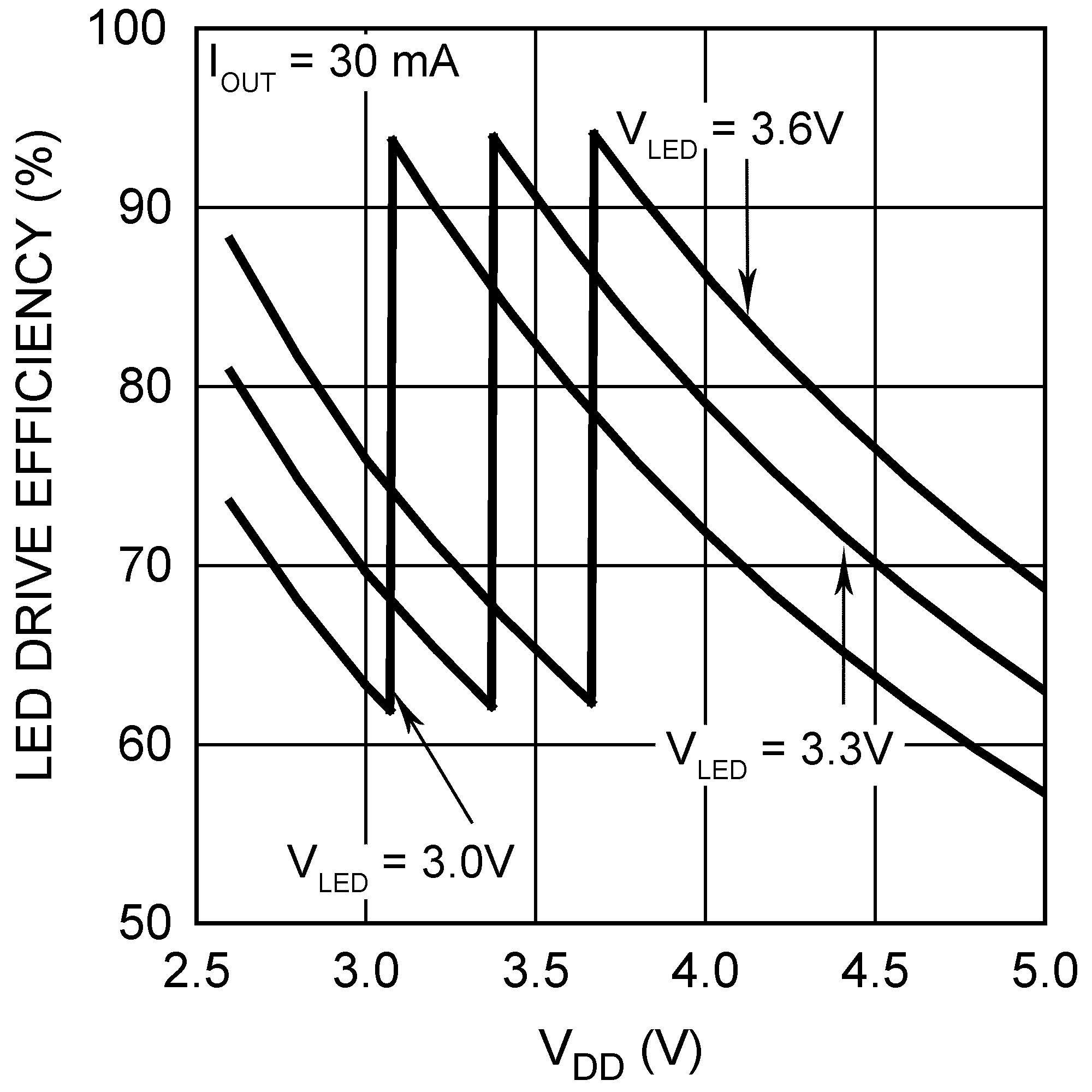 Figure 2. LED Drive Efficiency vs Input Voltage Automatic Gain Change
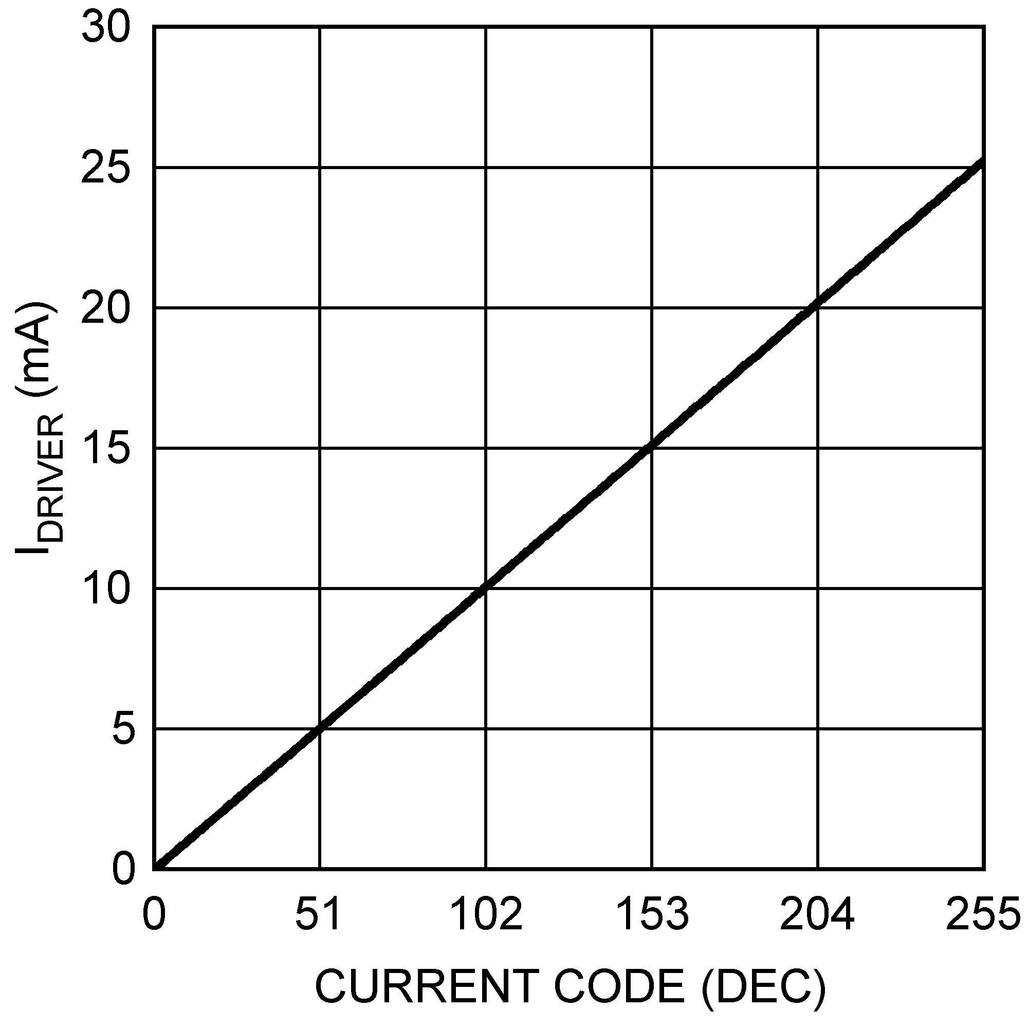 Figure 4. LED Current vs Current Register Code
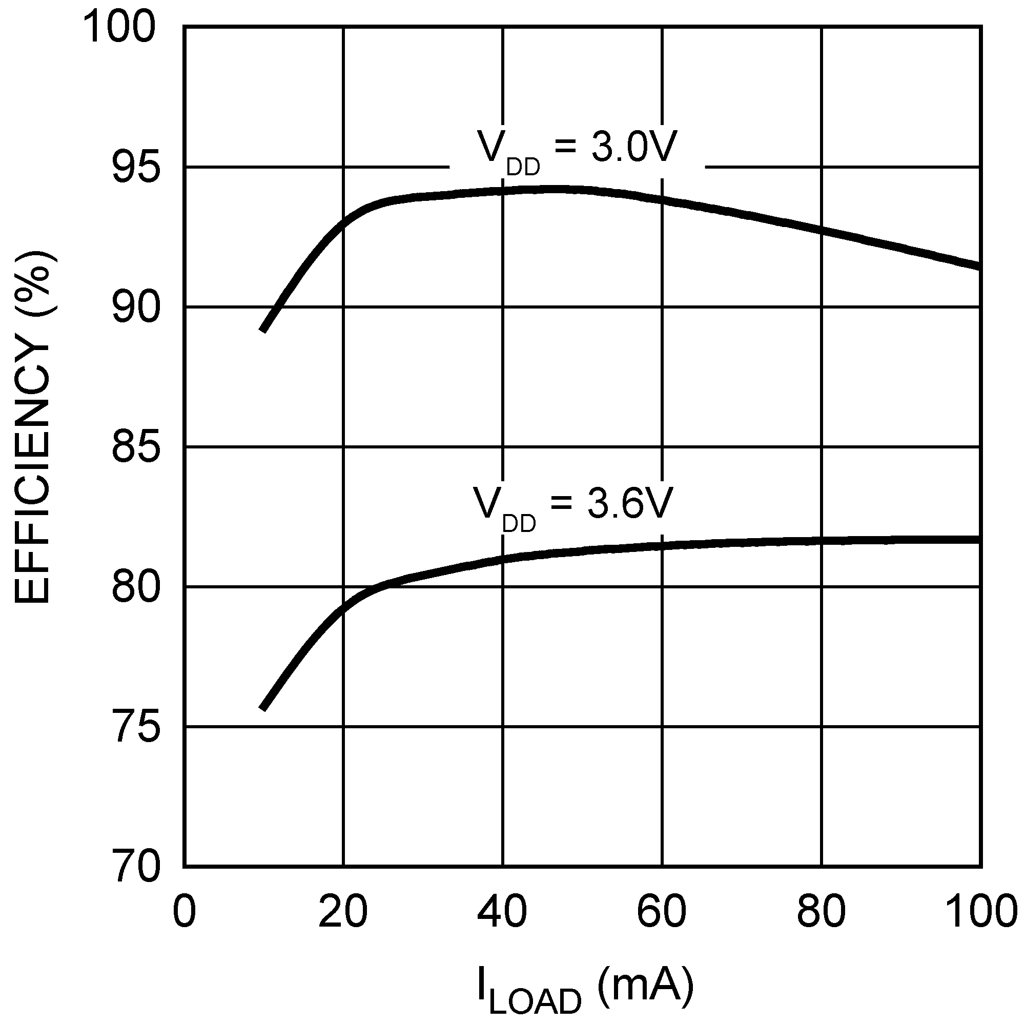 Figure 6. Charge Pump Efficiency vs Load Current
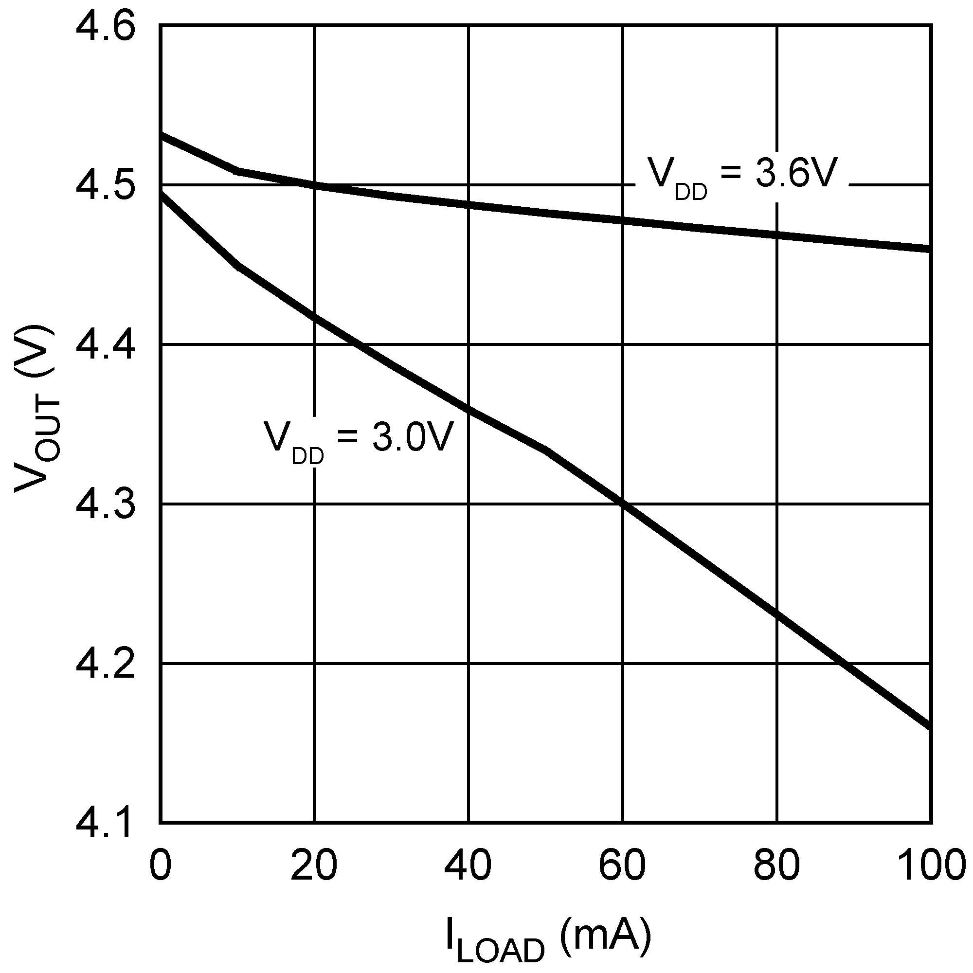 Figure 8. Charge Pump Output Voltage vs Load Current
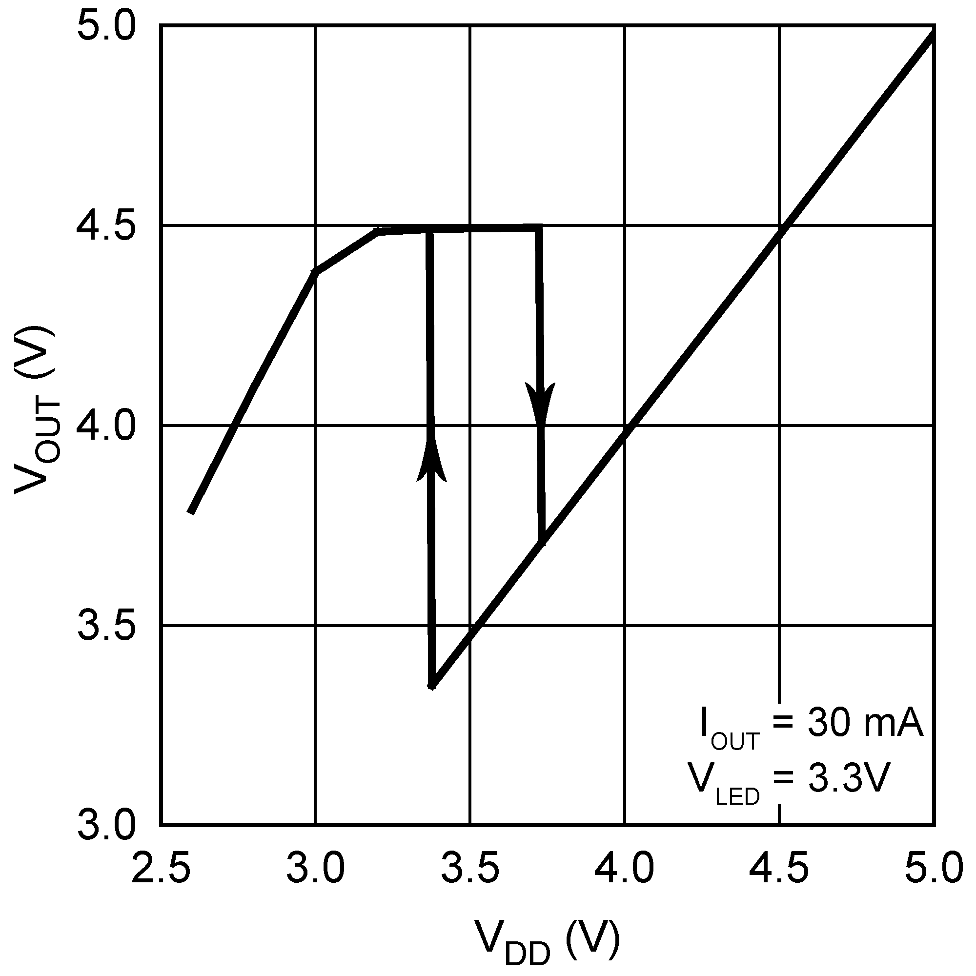 Figure 10. Charge Pump Automatic Gain Change Hysteresis
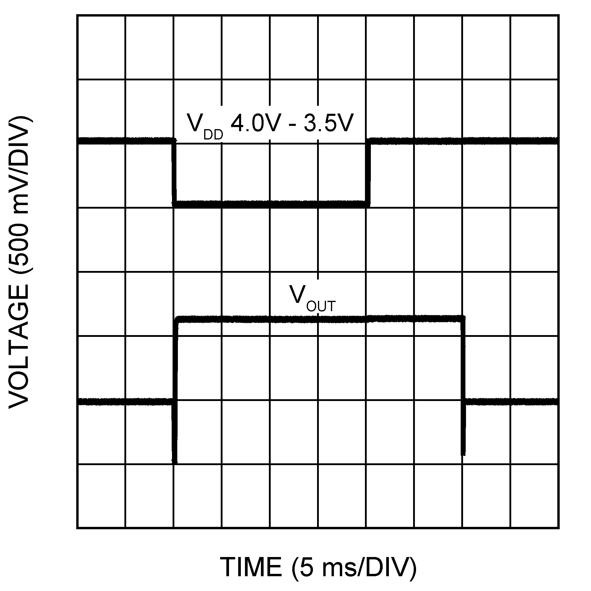 Figure 12. Charge Pump Automatic Gain Change
 (LED VF = 3.6 V)
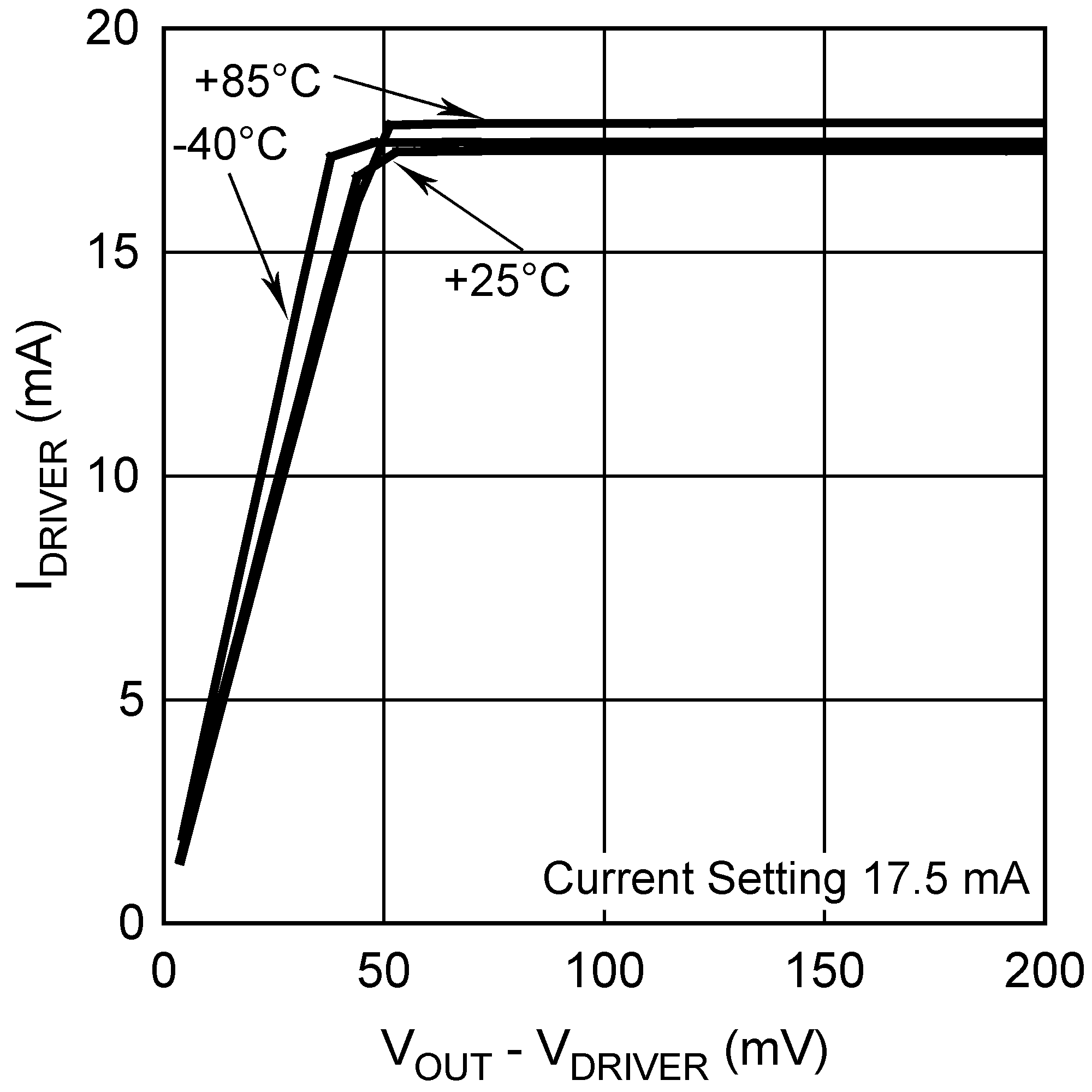 Figure 3. LED Current vs Output Pin Headroom Voltage
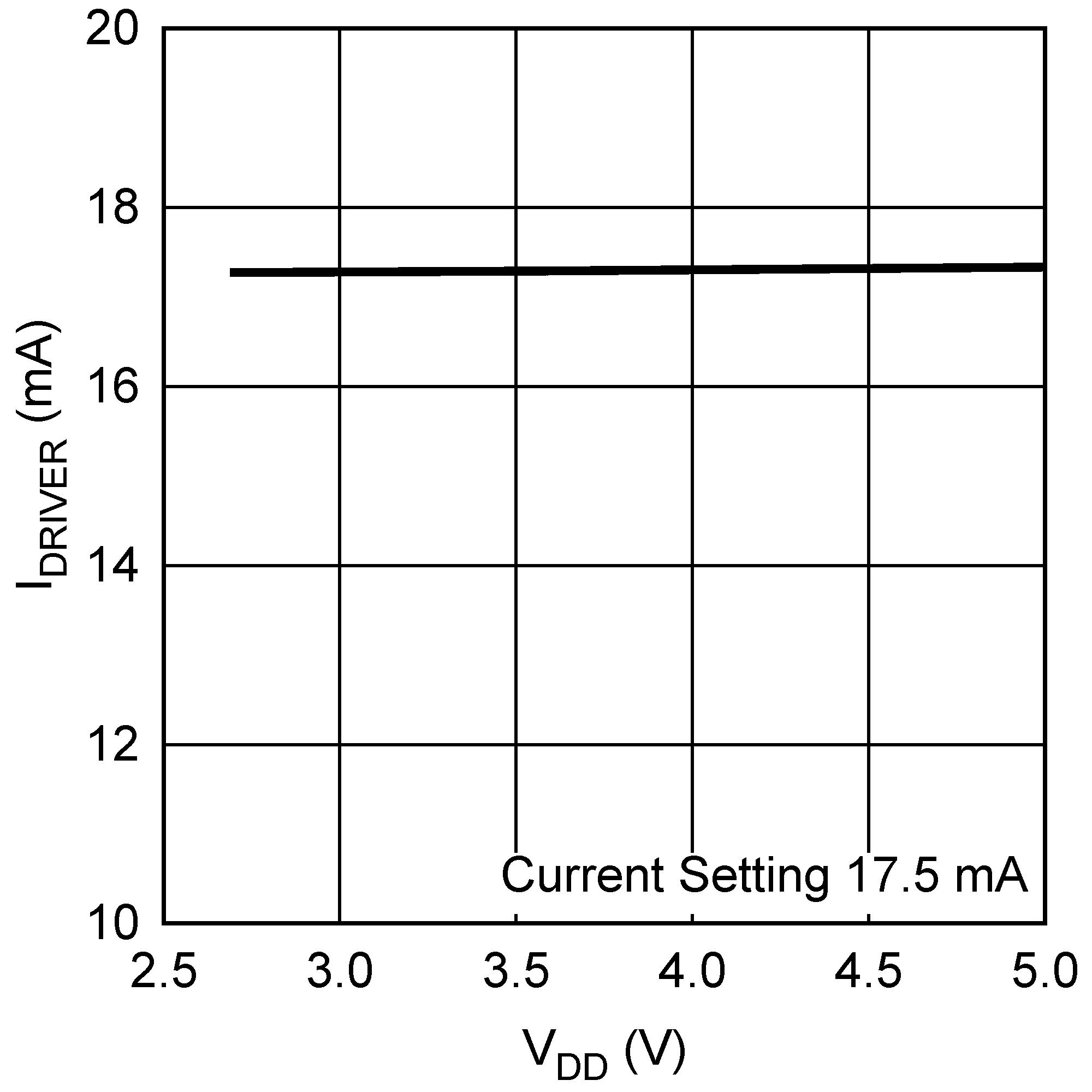 Figure 5. LED Current vs Supply Voltage
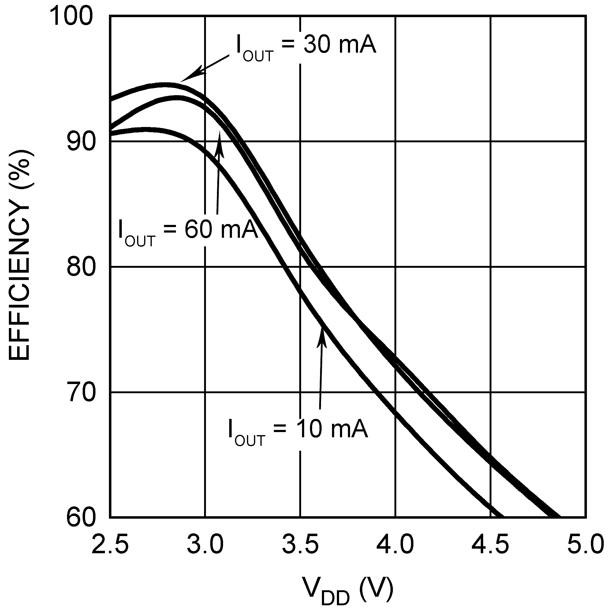 Figure 7. Charge Pump Efficiency vs Input Voltage 1.5x Mode
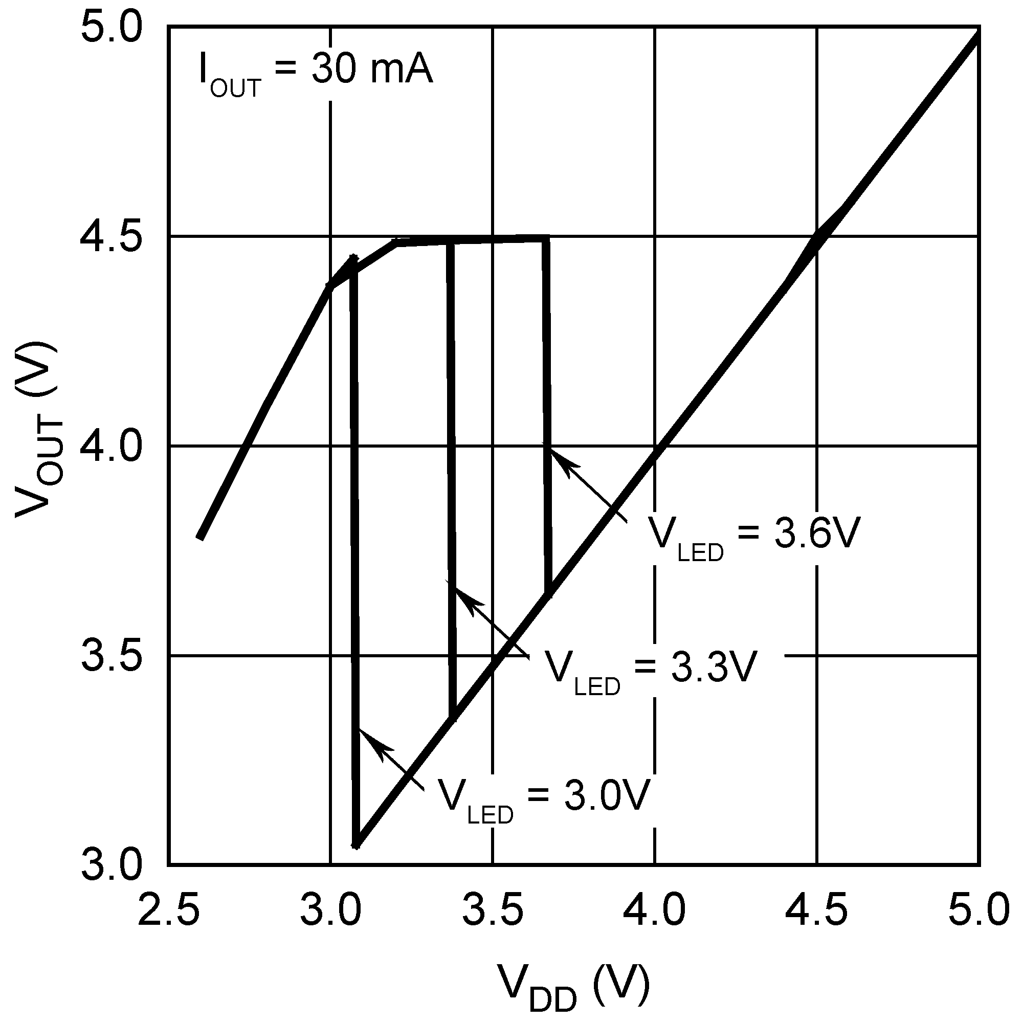 Figure 9. Charge Pump Output Voltage vs Input Voltage
Automatic Gain Change from 1x to 1.5x
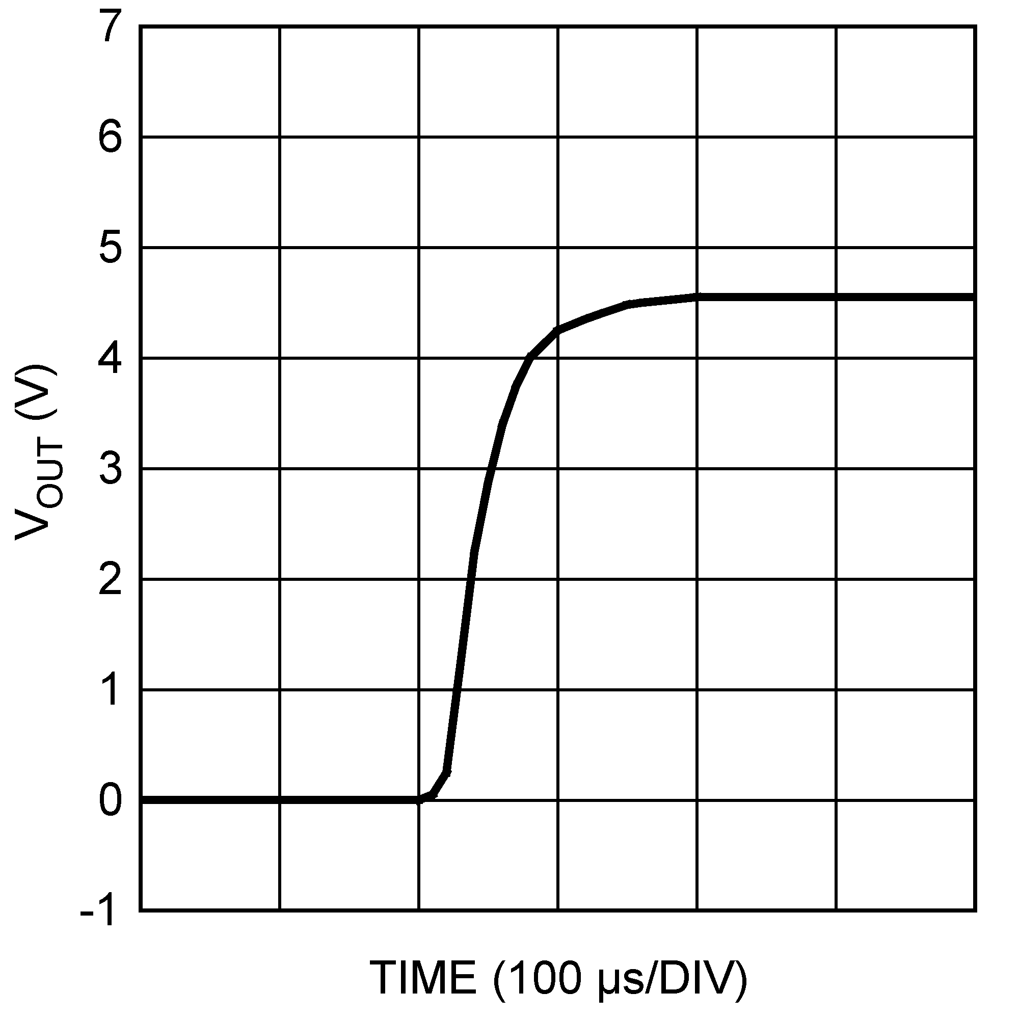 Figure 11. Charge Pump Start-Up in 1.5× Mode: No Load
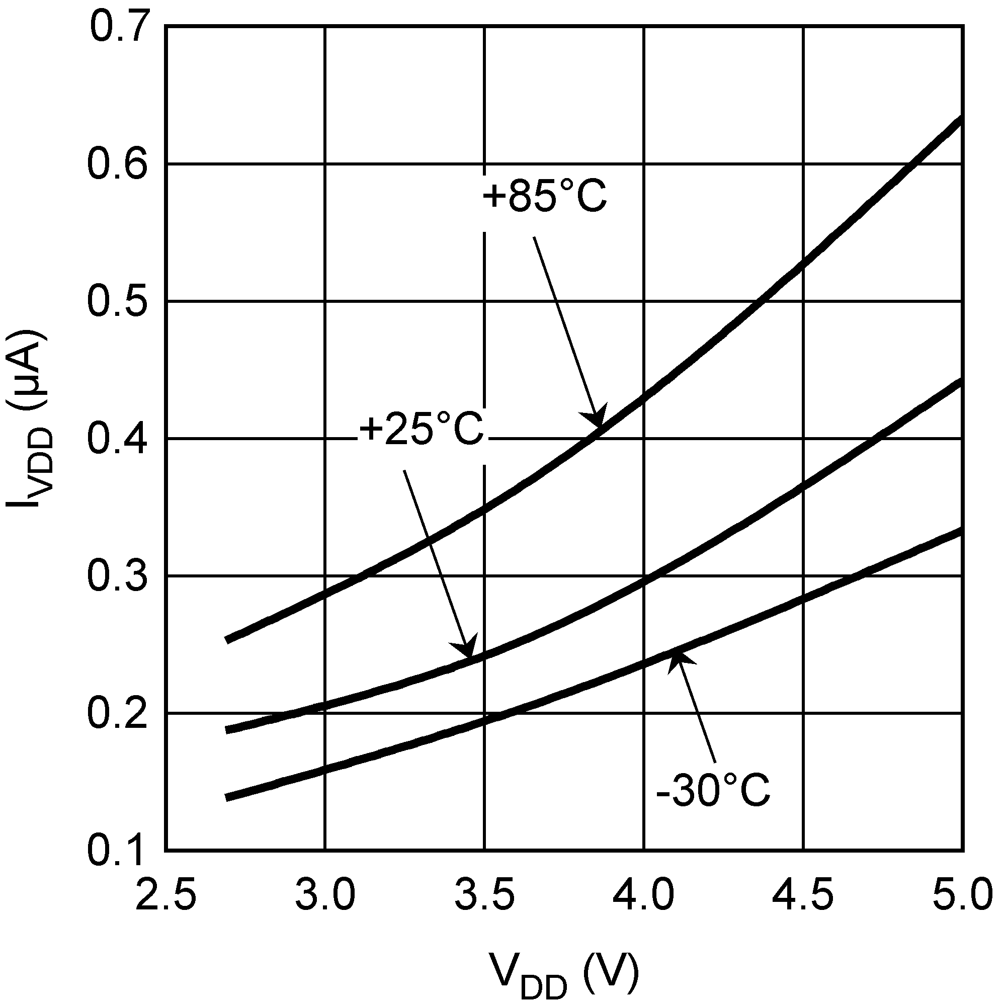 Figure 13. Standby Current vs Input Voltage