ZHCSD18A March   2013  – October 2014 LP55231

PRODUCTION DATA.  

  1. 特性
  2. 应用
  3. 说明
  4. 修订历史记录
  5. Pin Configuration and Functions
  6. Specifications
    1. 6.1  Absolute Maximum Ratings
    2. 6.2  Handling Ratings
    3. 6.3  Recommended Operating Conditions
    4. 6.4  Thermal Information
    5. 6.5  Electrical Characteristics
    6. 6.6  Charge Pump Electrical Characteristics
    7. 6.7  LED Driver Electrical Characteristics
    8. 6.8  LED Test Electrical Characteristics
    9. 6.9  Logic Interface Characteristics
    10. 6.10 Recommended External Clock Source Conditions
    11. 6.11 Serial Bus Timing Parameters (SDA, SCL)
    12. 6.12 Typical Characteristics
  7. Detailed Description
    1. 7.1 Overview
    2. 7.2 Functional Block Diagram
    3. 7.3 Feature Description
      1. 7.3.1 Programming
      2. 7.3.2 LED Error Detection
      3. 7.3.3 Energy Efficiency
      4. 7.3.4 Temperature Compensation
      5. 7.3.5 Charge Pump Operational Description
        1. 7.3.5.1 Overview
        2. 7.3.5.2 Output Resistance
        3. 7.3.5.3 Controlling The Charge Pump
        4. 7.3.5.4 LED Forward Voltage Monitoring
        5. 7.3.5.5 Gain Change Hysteresis
      6. 7.3.6 LED Driver Operational Description
        1. 7.3.6.1 Overview
        2. 7.3.6.2 Powering LEDs
        3. 7.3.6.3 Controlling The High-Side LED Drivers
      7. 7.3.7 Automatic Power-Save Mode
      8. 7.3.8 PWM Power-Save Mode
    4. 7.4 Device Functional Modes
      1. 7.4.1 Modes Of Operation
    5. 7.5 Programming
      1. 7.5.1 I2C-Compatible Control Interface
        1. 7.5.1.1 Data Validity
        2. 7.5.1.2 Start And Stop Conditions
        3. 7.5.1.3 Transferring Data
      2. 7.5.2 I2C-Compatible Chip Address
        1. 7.5.2.1 Control Register Write Cycle
        2. 7.5.2.2 Control Register Read Cycle
        3. 7.5.2.3 Auto-Increment Feature
    6. 7.6 Register Maps
      1. 7.6.1 Register Set
      2. 7.6.2 Control Register Details
      3. 7.6.3 Instruction Set
      4. 7.6.4 LED Driver Instructions
        1. 7.6.4.1 Ramp
        2. 7.6.4.2 Ramp Instruction Application Example
        3. 7.6.4.3 Set_PWM
        4. 7.6.4.4 Wait
      5. 7.6.5 LED Mapping Instructions
        1. 7.6.5.1  MUX_LD_START; MUX_LD_END
        2. 7.6.5.2  MUX_MAP_START
        3. 7.6.5.3  MUX_SEL
        4. 7.6.5.4  MUX_CLR
        5. 7.6.5.5  MUX_MAP_NEXT
        6. 7.6.5.6  MUX_LD_NEXT
        7. 7.6.5.7  MUX_MAP_PREV
        8. 7.6.5.8  MUX_LD_PREV
        9. 7.6.5.9  MUX_MAP_ADDR
        10. 7.6.5.10 MUX_LD_ADDR
      6. 7.6.6 Branch Instructions
        1. 7.6.6.1 BRANCH
        2. 7.6.6.2 INT
        3. 7.6.6.3 RST
        4. 7.6.6.4 END
        5. 7.6.6.5 TRIGGER
      7. 7.6.7 Arithmetic Instructions
        1. 7.6.7.1 LD
        2. 7.6.7.2 ADD
        3. 7.6.7.3 SUB
  8. Application and Implementation
    1. 8.1 Application Information
    2. 8.2 Typical Applications
      1. 8.2.1 Using Two LP55231 in the Same Application
        1. 8.2.1.1 Design Requirements
        2. 8.2.1.2 Detailed Design Procedure
        3. 8.2.1.3 Application Curves
      2. 8.2.2 Driving Haptic Feedback with LP55231
        1. 8.2.2.1 Design Requirements
        2. 8.2.2.2 Detailed Design Procedure
        3. 8.2.2.3 Application Curves
  9. Power Supply Recommendations
  10. 10Layout
    1. 10.1 Layout Guidelines
    2. 10.2 Layout Example
  11. 11器件和文档支持
    1. 11.1 器件支持
      1. 11.1.1 第三方米6体育平台手机版_好二三四免责声明
    2. 11.2 商标
    3. 11.3 静电放电警告
    4. 11.4 术语表
  12. 12机械封装和可订购信息

封装选项

机械数据 (封装 | 引脚)
散热焊盘机械数据 (封装 | 引脚)
订购信息

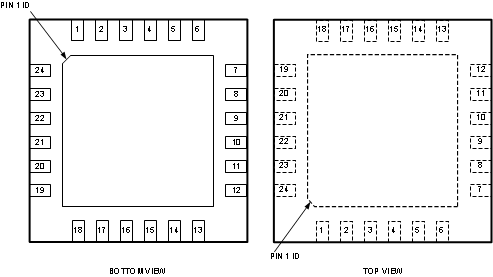
5 Pin Configuration and Functions

WQFN (RTW)
24 Pins
30198602.gif

Pin Functions

PIN TYPE(1) DESCRIPTION
NUMBER NAME
1 C2+ A Flying capacitor 2 positive terminal
2 C1+ A Flying capacitor 1 positive terminal
3 VDD P Input power supply
4 GND G Ground
5 EN I Enable
6 CLK I 32 kHz clock input. Connect to ground if not used
7 INT OD/O Interrupt for microcontroller unit. Leave unconnected if not used
8 SDA I/OD Serial interface data
9 SCL I Serial interface clock
10 TRIG I/OD Trigger. Connect to ground if not used
11 D9 A Current source output 9.
Note: powered from VDD
12 D8 A Current source output 8.
Note: powered from VDD
13 D7 A Current source output 7.
Note: powered from VDD
14 D6 A Current source output 6
15 D5 A Current source output 5
16 D4 A Current source output 4
17 D3 A Current source output 3
18 D2 A Current source output 2
19 D1 A Current source output 1
20 ASEL0 I Serial interface address select input
21 ASEL1 I Serial interface address select input
22 VOUT A Charge pump output
23 C2− A Flying capacitor 2 negative terminal
24 C1− A Flying capacitor 1 negative terminal
DAP Connect the die attach pad to GND
(1) A: Analog Pin; G: Ground Pin; P: Power Pin; I: Input Pin; I/O Input/Output Pin; O: Output Pin; OD: Open Drain Pin