ZHCSGU2A July 2017 – September 2017 LP5569
PRODUCTION DATA.
- 1 特性
- 2 应用
- 3 说明
- 4 修订历史记录
- 5 Device Comparison Table
- 6 Pin Configuration and Functions
-
7 Specifications
- 7.1 Absolute Maximum Ratings
- 7.2 ESD Ratings
- 7.3 Recommended Operating Conditions
- 7.4 Thermal Information
- 7.5 Electrical Characteristics
- 7.6 Charge-Pump Electrical Characteristics
- 7.7 LED Current Sinks Electrical Characteristics
- 7.8 Logic Interface Characteristics
- 7.9 Timing Requirements (EN/PWM)
- 7.10 Serial-Bus Timing Requirements (SDA, SCL), See
- 7.11 External Clock Timing Requirements (CLK), See
- 7.12 Typical Characteristics
-
8 Detailed Description
- 8.1 Overview
- 8.2 Functional Block Diagram
- 8.3 Feature Description
- 8.4 Device Functional Modes
- 8.5 Programming
- 8.6
Register Maps
- 8.6.1
LP5569_MAP Registers
- 8.6.1.1 CONFIG Register (Address = 0h) [reset = 0h]
- 8.6.1.2 LED_ENGINE_CONTROL1 Register (Address = 1h) [reset = 0h]
- 8.6.1.3 LED_ENGINE_CONTROL2 Register (Address = 2h) [reset = 0h]
- 8.6.1.4 LED0_CONTROL Register (Address = 7h) [reset = 0h]
- 8.6.1.5 LED1_CONTROL Register (Address = 8h) [reset = 0h]
- 8.6.1.6 LED2_CONTROL Register (Address = 9h) [reset = 0h]
- 8.6.1.7 LED3_CONTROL Register (Address = Ah) [reset = 0h]
- 8.6.1.8 LED4_CONTROL Register (Address = Bh) [reset = 0h]
- 8.6.1.9 LED5_CONTROL Register (Address = Ch) [reset = 0h]
- 8.6.1.10 LED6_CONTROL Register (Address = Dh) [reset = 0h]
- 8.6.1.11 LED7_CONTROL Register (Address = Eh) [reset = 0h]
- 8.6.1.12 LED8_CONTROL Register (Address = Fh) [reset = 0h]
- 8.6.1.13 LED0_PWM Register (Address = 16h) [reset = 0h]
- 8.6.1.14 LED1_PWM Register (Address = 17h) [reset = 0h]
- 8.6.1.15 LED2_PWM Register (Address = 18h) [reset = 0h]
- 8.6.1.16 LED3_PWM Register (Address = 19h) [reset = 0h]
- 8.6.1.17 LED4_PWM Register (Address = 1Ah) [reset = 0h]
- 8.6.1.18 LED5_PWM Register (Address = 1Bh) [reset = 0h]
- 8.6.1.19 LED6_PWM Register (Address = 1Ch) [reset = 0h]
- 8.6.1.20 LED7_PWM Register (Address = 1Dh) [reset = 0h]
- 8.6.1.21 LED8_PWM Register (Address = 1Eh) [reset = 0h]
- 8.6.1.22 LED0_CURRENT Register (Address = 22h) [reset = AFh]
- 8.6.1.23 LED1_CURRENT Register (Address = 23h) [reset = AFh]
- 8.6.1.24 LED2_CURRENT Register (Address = 24h) [reset = AFh]
- 8.6.1.25 LED3_CURRENT Register (Address = 25h) [reset = AFh]
- 8.6.1.26 LED4_CURRENT Register (Address = 26h) [reset = AFh]
- 8.6.1.27 LED5_CURRENT Register (Address = 27h) [reset = AFh]
- 8.6.1.28 LED6_CURRENT Register (Address = 28h) [reset = AFh]
- 8.6.1.29 LED7_CURRENT Register (Address = 29h) [reset = AFh]
- 8.6.1.30 LED8_CURRENT Register (Address = 2Ah) [reset = AFh]
- 8.6.1.31 MISC Register (Address = 2Fh) [reset = 40h]
- 8.6.1.32 ENGINE1_PC Register (Address = 30h) [reset = 0h]
- 8.6.1.33 ENGINE2_PC Register (Address = 31h) [reset = 0h]
- 8.6.1.34 ENGINE3_PC Register (Address = 32h) [reset = 0h]
- 8.6.1.35 MISC2 Register (Address = 33h) [reset = 2h]
- 8.6.1.36 ENGINE_STATUS Register (Address = 3Ch) [reset = 80h]
- 8.6.1.37 IO_CONTROL Register (Address = 3Dh) [reset = 2h]
- 8.6.1.38 VARIABLE_D Register (Address = 3Eh) [reset = 0h]
- 8.6.1.39 RESET Register (Address = 3Fh) [reset = 0h]
- 8.6.1.40 ENGINE1_VARIABLE_A Register (Address = 42h) [reset = 0h]
- 8.6.1.41 ENGINE2_VARIABLE_A Register (Address = 43h) [reset = 0h]
- 8.6.1.42 ENGINE3_VARIABLE_A Register (Address = 44h) [reset = 0h]
- 8.6.1.43 MASTER_FADER1 Register (Address = 46h) [reset = 0h]
- 8.6.1.44 MASTER_FADER2 Register (Address = 47h) [reset = 0h]
- 8.6.1.45 MASTER_FADER3 Register (Address = 48h) [reset = 0h]
- 8.6.1.46 MASTER_FADER_PWM Register (Address = 4Ah) [reset = 0h]
- 8.6.1.47 ENGINE1_PROG_START Register (Address = 4Bh) [reset = 0h]
- 8.6.1.48 ENGINE2_PROG_START Register (Address = 4Ch) [reset = 0h]
- 8.6.1.49 ENGINE3_PROG_START Register (Address = 4Dh) [reset = 0h]
- 8.6.1.50 PROG_MEM_PAGE_SELECT Register (Address = 4Fh) [reset = 0h]
- 8.6.1.51 PROGRAM_MEM_00 Register (Address = 50h) [reset = 0h]
- 8.6.1.52 PROGRAM_MEM_01 Register (Address = 51h) [reset = 0h]
- 8.6.1.53 PROGRAM_MEM_02 Register (Address = 52h) [reset = 0h]
- 8.6.1.54 PROGRAM_MEM_03 Register (Address = 53h) [reset = 0h]
- 8.6.1.55 PROGRAM_MEM_04 Register (Address = 54h) [reset = 0h]
- 8.6.1.56 PROGRAM_MEM_05 Register (Address = 55h) [reset = 0h]
- 8.6.1.57 PROGRAM_MEM_06 Register (Address = 56h) [reset = 0h]
- 8.6.1.58 PROGRAM_MEM_07 Register (Address = 57h) [reset = 0h]
- 8.6.1.59 PROGRAM_MEM_08 Register (Address = 58h) [reset = 0h]
- 8.6.1.60 PROGRAM_MEM_09 Register (Address = 59h) [reset = 0h]
- 8.6.1.61 PROGRAM_MEM_10 Register (Address = 5Ah) [reset = 0h]
- 8.6.1.62 PROGRAM_MEM_11 Register (Address = 5Bh) [reset = 0h]
- 8.6.1.63 PROGRAM_MEM_12 Register (Address = 5Ch) [reset = 0h]
- 8.6.1.64 PROGRAM_MEM_13 Register (Address = 5Dh) [reset = 0h]
- 8.6.1.65 PROGRAM_MEM_14 Register (Address = 5Eh) [reset = 0h]
- 8.6.1.66 PROGRAM_MEM_15 Register (Address = 5Fh) [reset = 0h]
- 8.6.1.67 PROGRAM_MEM_16 Register (Address = 60h) [reset = 0h]
- 8.6.1.68 PROGRAM_MEM_17 Register (Address = 61h) [reset = 0h]
- 8.6.1.69 PROGRAM_MEM_18 Register (Address = 62h) [reset = 0h]
- 8.6.1.70 PROGRAM_MEM_19 Register (Address = 63h) [reset = 0h]
- 8.6.1.71 PROGRAM_MEM_20 Register (Address = 64h) [reset = 0h]
- 8.6.1.72 PROGRAM_MEM_21 Register (Address = 65h) [reset = 0h]
- 8.6.1.73 PROGRAM_MEM_22 Register (Address = 66h) [reset = 0h]
- 8.6.1.74 PROGRAM_MEM_23 Register (Address = 67h) [reset = 0h]
- 8.6.1.75 PROGRAM_MEM_24 Register (Address = 68h) [reset = 0h]
- 8.6.1.76 PROGRAM_MEM_25 Register (Address = 69h) [reset = 0h]
- 8.6.1.77 PROGRAM_MEM_26 Register (Address = 6Ah) [reset = 0h]
- 8.6.1.78 PROGRAM_MEM_27 Register (Address = 6Bh) [reset = 0h]
- 8.6.1.79 PROGRAM_MEM_28 Register (Address = 6Ch) [reset = 0h]
- 8.6.1.80 PROGRAM_MEM_29 Register (Address = 6Dh) [reset = 0h]
- 8.6.1.81 PROGRAM_MEM_30 Register (Address = 6Eh) [reset = 0h]
- 8.6.1.82 PROGRAM_MEM_31 Register (Address = 6Fh) [reset = 0h]
- 8.6.1.83 ENGINE1_MAPPING1 Register (Address = 70h) [reset = 0h]
- 8.6.1.84 ENGINE1_MAPPING2 Register (Address = 71h) [reset = 0h]
- 8.6.1.85 ENGINE2_MAPPING1 Register (Address = 72h) [reset = 0h]
- 8.6.1.86 ENGINE2_MAPPING2 Register (Address = 73h) [reset = 0h]
- 8.6.1.87 ENGINE3_MAPPING1 Register (Address = 74h) [reset = 0h]
- 8.6.1.88 ENGINE3_MAPPING2 Register (Address = 75h) [reset = 0h]
- 8.6.1.89 PWM_CONFIG Register (Address = 80h) [reset = 4h]
- 8.6.1.90 LED_FAULT1 Register (Address = 81h) [reset = 0h]
- 8.6.1.91 LED_FAULT2 Register (Address = 82h) [reset = 0h]
- 8.6.1.92 GENERAL_FAULT Register (Address = 83h) [reset = 4h]
- 8.6.1
LP5569_MAP Registers
- 9 Application and Implementation
- 10Power Supply Recommendations
- 11Layout
- 12器件和文档支持
- 13机械、封装和可订购信息
9 Application and Implementation
NOTE
Information in the following applications sections is not part of the TI component specification, and TI does not warrant its accuracy or completeness. TI’s customers are responsible for determining suitability of components for their purposes. Customers should validate and test their design implementation to confirm system functionality.
9.1 Application Information
The LP5569 device is designed as an autonomous lighting controller for handheld devices. In these devices, extremely small form factor is needed; therefore, the LP5569 device is designed to require only four small capacitors: input and output, as well as flying capacitor 1 and flying capacitor 2 for the charge pump. If the system has other LED input voltages available, and the charge pump is not needed in the application, the charge-pump capacitors can be omitted, thus reducing the solution even further. The device can drive RGB LEDs or discrete LEDs of any color if desired.
9.2 Typical Applications
9.2.1 Single LP5569 Application
Figure 119 shows an example of a typical application that uses a charge pump to get high-enough voltage to drive green and blue LEDs. Red LEDs are powered from VVIN for reduced power consumption. The device, with a voltage range of 2.5 V to 4.5 V, is powered from three AA batteries, typically 3.6 V with 1.2-V cell voltage. Design Requirements shows related design parameters for this example. In this example, input voltage with AA batteries is typically over 3.6 V (cell voltage >1.2 V) for half of the battery lifetime. During this time the charge pump operates in 1× mode, as the input voltage is enough for the green and blue LEDs. As the battery voltage continues to decrease, the LP5569 device detects that the LED headroom voltage is too low and automatically configures the charge pump to the 1.5× mode. In 1.5× mode, the LEDs can be powered with VIN down to 2.5 V, where the batteries are almost empty.
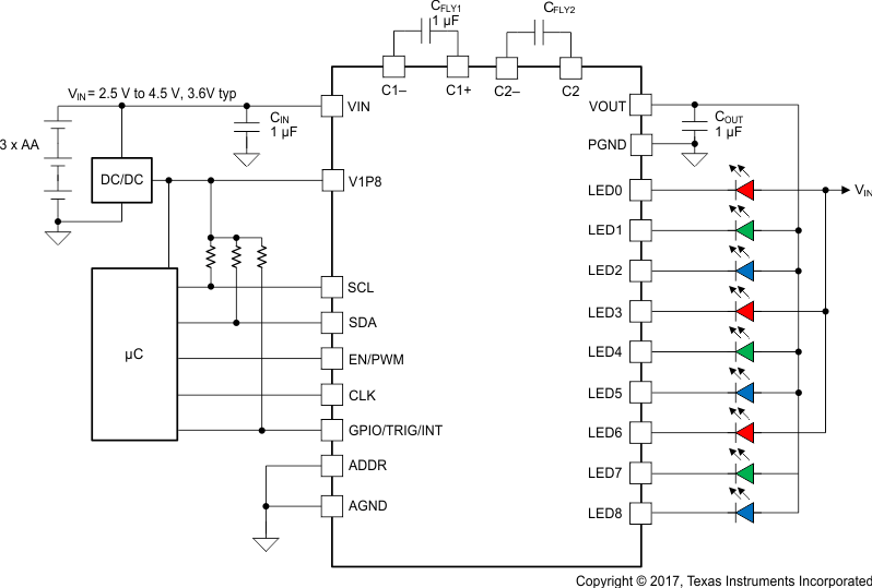 Figure 119. LP5569 Typical Application
9.2.1.1 Design Requirements
| DESIGN PARAMETER | EXAMPLE VALUE | |||
|---|---|---|---|---|
| Input voltage range | 2.5 V to 5.5 V | |||
| LED VF (maximum) | 3.2 V | |||
| LED current | 25.5 mA maximum | |||
| Input capacitor | CIN = 1 µF | |||
| Output capacitor | COUT = 1 µF | |||
| Charge pump flying capacitors | CFLY1 = CFLY2 = 1 µF | |||
| Charge-pump mode | 1.5× or automatic | |||
9.2.1.2 Detailed Design Procedure
The LP5569 device requires four external capacitors for proper operation. TI recommends surface-mount multi-layer ceramic capacitors. Tantalum and aluminum capacitors are not recommended because of their high ESR. Multi-layer ceramic capacitors must always be used for the flying capacitors (CFLY1 and CFLY2). Ceramic capacitors with an X7R or X5R temperature characteristic are preferred for use with the LP5569 device. These capacitors have tight capacitance tolerance (as good as ±10%) and hold their value over temperature (X7R: ±15% over −55°C to 125°C; X5R: ±15% over −55°C to 85°C).
It is necessary to have at least 0.24 μF of effective capacitance for each of the flying capacitors under all operating conditions to ensure proper operation. The output capacitor COUT directly affects the magnitude of the output ripple voltage. In general, the higher the value of COUT, the lower the output-ripple magnitude. For proper operation TI recommends having at least 0.5 μF of effective capacitance for CIN and COUT under all operating conditions. The voltage rating of all four capacitors must be 6.3 V (minimum), with 10 V preferred.
Table 108 lists suitable external components from some leading ceramic capacitor manufacturers.
Table 108. Suitable External Components
| MODEL | TYPE | VENDOR | VOLTAGE RATING (V) | PACKAGE SIZE |
|---|---|---|---|---|
| C1005X5R1A105K | Ceramic X5R | TDK | 10 | 0402 |
| LMK105BJ105KV-F | Ceramic X5R | Taiyo Yuden | 10 | 0402 |
| ECJ0EB1A105M | Ceramic X5R | Panasonic | 10 | 0402 |
9.2.2 Using Multiple LP5569 Devices
The LP5569 device enables up to eight parallel devices together, which can drive up to 24 RGB LEDs or 72 single LEDs. Figure 122 shows the connections for two LP5569 devices for six RGB LEDs. Note that the LED6, LED7, and LED8 outputs are used for the red LEDs. The SCL and SDA lines must each have a pullup resistor placed somewhere on the line (R2 and R3; the pullup resistors are normally located on the bus master). In typical applications, values of 1.8 kΩ to 4.7 kΩ are used, depending on the bus capacitance, I/O voltage, and the desired communication speed. GPIO/TRIG/INT is open drain, which requires a pullup resistor. The typical value for R1 is from 120 kΩ to 180 kΩ for two LP5569 devices.
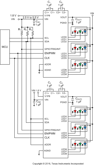 Figure 122. Dual LP5569 Application Example
9.2.2.1 Design Requirements
| DESIGN PARAMETER | EXAMPLE VALUE | |||
|---|---|---|---|---|
| Input voltage range | 2.5 V to 5.5 V | |||
| LED VF (maximum) | 3.2 V | |||
| LED current | 25.5 mA maximum | |||
| Input capacitor | CIN = 1 µF | |||
| Output capacitor | COUT= 1 µF | |||
| Charge pump flying capacitors | CFLY1 = CFLY2 = 1 µF | |||
| Charge-pump mode | 1.5× or automatic | |||
9.2.2.2 Detailed Design Procedure
External component selection follows the earlier example (see Detailed Design Procedure).
