ZHCSQG6A March 2022 – May 2022 LP5891
PRODUCTION DATA
- 1 特性
- 2 应用
- 3 说明
- 4 Revision History
- 5 Pin Configuration and Functions
- 6 Specifications
-
7 Detailed Description
- 7.1 Overview
- 7.2 Functional Block Diagram
- 7.3
Feature Description
- 7.3.1 Independent and Stackable Mode
- 7.3.2 Current Setting
- 7.3.3 Frequency Multiplier
- 7.3.4 Line Transitioning Sequence
- 7.3.5 Protections and Diagnostics
- 7.4 Device Functional Modes
- 7.5 Continuous Clock Series Interface
- 7.6 PWM Grayscale Control
- 7.7 Register Maps
- 8 Application and Implementation
- 9 Power Supply Recommendations
- 10Layout
- 11Device and Documentation Support
- 12Mechanical, Packaging, and Orderable Information
请参考 PDF 数据表获取器件具体的封装图。
机械数据 (封装 | 引脚)
- RRF|76
- ZXL|96
散热焊盘机械数据 (封装 | 引脚)
10.2 Layout Example
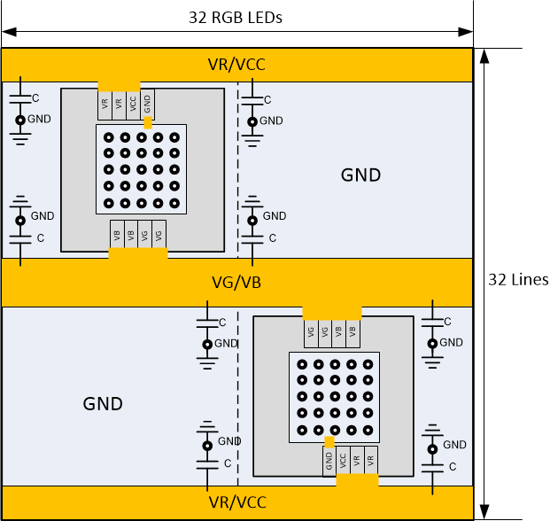
To simplify the system power rails design, VR, VCC must use one power rail and VG, VB use another power rail. Figure 10-1 gives an example for power rails routing.
Connect the GND pin to the thermal pad on the board with the shortest wire and the thermal pad is connected to GND plane with the vias, as many as possible to help the power dissipation.
 Figure 10-1 Power Rails Routing Suggestion
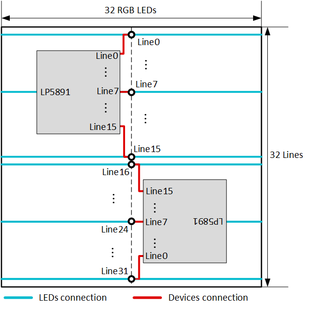
Figure 10-2 gives an example for line routing. Connect the line switch to the center of the line bus, so as to uniform the current flowing from the line switch to the left side and right side LEDs in white grayscale. With this connection, the unbalance of the parasitic inductor from the routing is the smallest and the display performance is better, especially in low grayscale condition.
 Figure 10-2 Line Routing
Suggestion
Figure 10-2 Line Routing
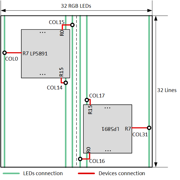
SuggestionFigure 10-3 gives an example for channel routing with the shortest wire. With this connection, the channel to the LED path is the shortest, which can reduce the wire inductance, and be a benefit to the performance. However, the data transmission sequence must be adjusted to follow the pins routing map. For example, R0 connects to column 15 (LED15 ). The first data must be column 15 (LED15) rather than column 0 (LED0).
 Figure 10-3 Channel Routing Suggestion with
Shortest Wire
Figure 10-3 Channel Routing Suggestion with
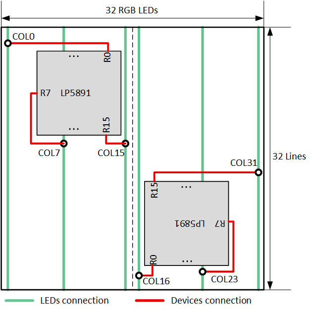
Shortest WireFigure 10-4 gives an example for channel routing with pin number sequence. With this connection, the data transmission sequence is the same with pin number sequence. For example, R0 connects to column 0 (LED0 ). The first data is column 0 (LED0). However, with this connection, the inductance for each channel can be different, which can bring a slight difference for the worst case.
 Figure 10-4 Channel Routing Suggestion with Channel Order
Sequence