SNVS358R July 2005 – June 2016 LP5900
PRODUCTION DATA.
- 1 Features
- 2 Applications
- 3 Description
- 4 Revision History
- 5 Pin Configuration and Functions
- 6 Specifications
- 7 Detailed Description
- 8 Application and Implementation
- 9 Power Supply Recommendations
- 10Layout
- 11Device and Documentation Support
- 12Mechanical, Packaging, and Orderable Information
封装选项
机械数据 (封装 | 引脚)
散热焊盘机械数据 (封装 | 引脚)
订购信息
5 Pin Configuration and Functions
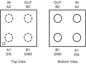
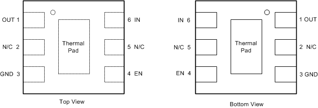
YZR and YPF Packages
4-Pin DSBGA

NGF Package
6-Pin WSON with Exposed Thermal Pad

Pin Functions
| PIN | TYPE | DESCRIPTION | ||
|---|---|---|---|---|
| DSBGA | WSON | NAME | ||
| A1 | 4 | EN | I | Enable input; disables the regulator when ≤ 0.4 V. Enables the regulator when ≥ 1.2 V. An internal 1-MΩ pull-down resistor connects this input to ground. |
| A2 | 6 | IN | I | Input voltage supply. Connect a 0.47-µF capacitor at this input. |
| B1 | 3 | GND | — | Common ground |
| B2 | 1 | OUT | O | Output voltage. A 0.47-μF Low ESR capacitor should be connected to this pin. Connect this output to the load circuit. |
| — | 2 | NC | — | No internal connection. |
| — | Thermal Pad | Thermal Pad | — | The exposed thermal pad on the bottom of the packagemust be connected to a copper area on the PCB under the package. TI recommends use of thermal vias to remove heat from the package into the PCB. Connect the thermal pad to ground potential or leave floating. Do not connect the thermal pad to any potential other than the same ground potential seen at device pin 3. For additional information on using TI's non-pullback WSON package, see AN-1187 Leadless Leadframe Package (LLP) (SNOA401). |