SNVS358R July 2005 – June 2016 LP5900
PRODUCTION DATA.
- 1 Features
- 2 Applications
- 3 Description
- 4 Revision History
- 5 Pin Configuration and Functions
- 6 Specifications
- 7 Detailed Description
- 8 Application and Implementation
- 9 Power Supply Recommendations
- 10Layout
- 11Device and Documentation Support
- 12Mechanical, Packaging, and Orderable Information
封装选项
机械数据 (封装 | 引脚)
散热焊盘机械数据 (封装 | 引脚)
订购信息
6 Specifications
6.1 Absolute Maximum Ratings
over operating free-air temperature range (unless otherwise noted)(1)(3)(2)| MIN | MAX | UNIT | |
|---|---|---|---|
| Input voltage, VIN | –0.3 | 6 | V |
| Output voltage, VOUT | –0.3 | VIN + 0.3 | |
| Enable input voltage, VEN | –0.3 | VIN + 0.3 | |
| Continuous power dissipation(4) | Internally Limited | ||
| Junction temperature, TJMAX | 150 | °C | |
| Storage temperature, Tstg | –65 | 150 | °C |
(1) Stresses beyond those listed under Absolute Maximum Ratings may cause permanent damage to the device. These are stress ratings only, which do not imply functional operation of the device at these or any other conditions beyond those indicated under Recommended Operating Conditions. Exposure to absolute-maximum-rated conditions for extended periods may affect device reliability.
(2) If Military/Aerospace specified devices are required, please contact the Texas Instruments Sales Office/ Distributors for availability and specifications.
(3) All voltages are with respect to the potential at the GND pin.
(4) Internal thermal shutdown circuitry protects the device from permanent damage.
6.2 ESD Ratings
| VALUE | UNIT | |||
|---|---|---|---|---|
| V(ESD) | Electrostatic discharge | Human-body model (HBM), per ANSI/ESDA/JEDEC JS-001(1) | ±2000 | V |
6.3 Recommended Operating Conditions
over operating free-air temperature range (unless otherwise noted)(1)| MIN | MAX | UNIT | |
|---|---|---|---|
| Input voltage, VIN | 2.5 | 5.5 | V |
| Enable voltage, VEN | 0 | VIN + 0.3 | V |
| Output current, IOUT(2) | 0 | 150 | mA |
| Junction temperature, TJ | –40 | 125 | °C |
| Ambient temperature, TA(2) | –40 | 85 | °C |
(1) All voltages are with respect to the potential at the GND pin.
(2) In applications where high power dissipation and/or poor package thermal resistance is present, the maximum ambient temperature may have to be derated. Maximum ambient temperature (TA-MAX) is dependent on the maximum operating junction temperature (TJ-MAX-OP = 125°C), the maximum power dissipation of the device in the application (PD-MAX), and the junction-to ambient thermal resistance of the part/package in the application (RθJA), as given by the following equation: TA-MAX = TJ-MAX-OP – (RθJA × PD-MAX). See Application and Implementation.
6.4 Thermal Information
| THERMAL METRIC(1) | LP5900 | UNIT | ||
|---|---|---|---|---|
| NGF | YZR/YPF | |||
| 6 PINS | 4 PINS | |||
| RθJA | Junction-to-ambient thermal resistance | 79.8 | 177.7 | °C/W |
| RθJC(top) | Junction-to-case (top) thermal resistance | 84.4 | 0.7 | °C/W |
| RθJB | Junction-to-board thermal resistance | 20.4 | 35.6 | °C/W |
| ψJT | Junction-to-top characterization parameter | 2.6 | 5.8 | °C/W |
| ψJB | Junction-to-board characterization parameter | 20.3 | 35.3 | °C/W |
| RθJC(bot) | Junction-to-case (bottom) thermal resistance | 11.2 | — | °C/W |
(1) For more information about traditional and new thermal metrics, see the Semiconductor and IC Package Thermal Metrics application report, SPRA953.
6.5 Electrical Characteristics
Unless otherwise noted, specifications apply in Figure 16 with: VIN = VOUT (NOM) + 1 V, VEN = 1.2 V, CIN = COUT = 0.47 μF, IOUT = 1 mA.(1)(2)| PARAMETER | TEST CONDITIONS | MIN | TYP | MAX | UNIT | ||
|---|---|---|---|---|---|---|---|
| VIN | Input voltage | 2.5 | 5.5 | V | |||
| ΔVOUT | Output voltage tolerance | VIN = (VOUT(NOM) + 1 V) to 5.5 V, IOUT = 1 mA to 150 mA, –40°C ≤ TJ ≤ 125°C |
−2% | 2% | |||
| Line regulation | VIN = (VOUT(NOM) + 1 V) to 5.5 V, IOUT = 1 mA | 0.05 | %V | ||||
| Load regulation | IOUT = 1 mA to 150 mA | 0.001 | %mA | ||||
| ILOAD | Load current | See(3) | mA | ||||
| Maximum output current | –40°C ≤ TJ ≤ 125°C | 150 | |||||
| IQ | Quiescent current(4) | VEN = 1.2 V, IOUT = 0 mA | 25 | µA | |||
| VEN = 1.2 V, IOUT = 0 mA, –40°C ≤ TJ ≤ 125°C | 50 | ||||||
| VEN = 1.2 V, IOUT = 150 mA | 160 | ||||||
| VEN = 1.2 V, IOUT = 150 mA, –40°C ≤ TJ ≤ 125°C | 230 | ||||||
| VEN = 0.3 V (disabled) | 0.003 | ||||||
| VEN = 0.3 V (disabled, –40°C ≤ TJ ≤ 125°C | 1 | ||||||
| IG | Ground current(5) | IOUT = 0 mA (VOUT = 2.5 V) | 30 | µA | |||
| VDO | Dropout voltage(6) | IOUT = 150 mA | 80 | mV | |||
| IOUT = 150 mA, –40°C ≤ TJ ≤ 125°C | 150 | ||||||
| ISC | Short-circuit current limit(7) | 300 | mA | ||||
| PSRR | Power supply rejection ratio(8) | f = 100 Hz, IOUT = 150 mA | 85 | dB | |||
| f = 1 kHz, IOUT = 150 mA | 75 | ||||||
| f = 10 kHz, IOUT = 150 mA | 65 | ||||||
| f = 50 kHz, IOUT = 150 mA | 52 | ||||||
| f = 100 kHz, IOUT = 150 mA | 40 | ||||||
| en | Output noise voltage(8) | BW = 10 Hz to 100 kHz, VIN = 4.2 V | IOUT = 0 mA | 7 | μVRMS | ||
| IOUT = 1 mA | 10 | ||||||
| IOUT = 150 mA | 6.5 | ||||||
| TSHUTDOWN | Thermal shutdown | Temperature | 160 | ºC | |||
| Hysteresis | 20 | ||||||
| LOGIN INPUT THRESHOLDS | |||||||
| VIL | Low input threshold (VEN) | VIN = 2.5 V to 5.5 V, –40°C ≤ TJ ≤ 125°C | 0.4 | V | |||
| VIH | High input threshold (VEN) | VIN = 2.5 V to 5.5 V, –40°C ≤ TJ ≤ 125°C | 1.2 | V | |||
| IEN | Input current at EN pin(9) | VEN = 5.5 V and VIN = 5.5 V | 5.5 | μA | |||
| VEN = 0 V and VIN = 5.5 V | 0.001 | ||||||
| TRANSIENT CHARACTERISTICS | |||||||
| ΔVOUT | Line transient(8) | VIN = (VOUT(NOM) + 1 V) to (VOUT(NOM) + 1.6 V) in 30 μs, IOUT = 1 mA, –40°C ≤ TJ ≤ 125°C | −2 | mV | |||
| VIN = (VOUT(NOM) + 1.6 V) to (VOUT(NOM) + 1 V) in 30 μs, IOUT = 1 mA, –40°C ≤ TJ ≤ 125°C | 2 | ||||||
| Load transient(8) | IOUT = 1 mA to 150 mA in 10 μs, –40°C ≤ TJ ≤ 125°C | −110 | mV | ||||
| IOUT = 150 mA to 1 mA in 10 μs, –40°C ≤ TJ ≤ 125°C | 50 | ||||||
| Overshoot on start-up(8) | –40°C ≤ TJ ≤ 125°C | 20 | mV | ||||
| Turnon time | To 95% of VOUT(NOM) | 150 | 300 | μs | |||
(1) All voltages are with respect to the potential at the GND pin.
(2) Minimum and Maximum limits are specified by design, test, or statistical analysis. Typical numbers are not ensured, but do represent the most likely norm.
(3) The device maintains a stable, regulated output voltage without a load current.
(4) Quiescent current is defined here as the difference in current between the input voltage source and the load at the OUT pin.
(5) Ground current is defined here as the total current flowing to ground as a result of all input voltages applied to the device.
(6) Dropout voltage is the voltage difference between the input and the output at which the output voltage drops to 100 mV below its nominal value. This parameter only applies to output voltages above 2.5 V.
(7) Short-circuit current is measured with OUT pulled to 0 V and IN worst case = 6 V.
(8) This specification is specified by design.
(9) There is a 1-MΩ resistor between EN pin and ground on the device.
6.6 Output and Input Capacitor, Recommended Specifications(1)
| PARAMETER | TEST CONDITIONS | MIN | NOM | MAX | UNIT | |
|---|---|---|---|---|---|---|
| CIN | Input capacitance | Capacitance for stability | 0.47 | µF | ||
| Capacitance for stability, –40°C ≤ TJ ≤ 125°C | 0.33 | |||||
| COUT | Output capacitance | Capacitance for stability | 0.47 | |||
| Capacitance for stability, –40°C ≤ TJ ≤ 125°C | 0.33 | 10 | ||||
| ESR | Output/Input capacitance | 5 | 500 | mΩ | ||
(1) The minimum capacitance must be greater than 0.33 µF over the full range of operating conditions. The capacitor tolerance must be 30% or better over the full temperature range. The full range of operating conditions for the capacitor in the application should be considered during device selection to ensure this minimum capacitance specification is met. TI recommends X7R capacitors; however, capacitor types X5R, Y5V and Z5U may be used with consideration of the application and conditions.
6.7 Typical Characteristics
Unless otherwise specified, CIN = COUT = 0.47 µF, VIN = VOUT(NOM) + 1 V, VEN = 1.2 V, IOUT = 1 mA , T A = 25°C.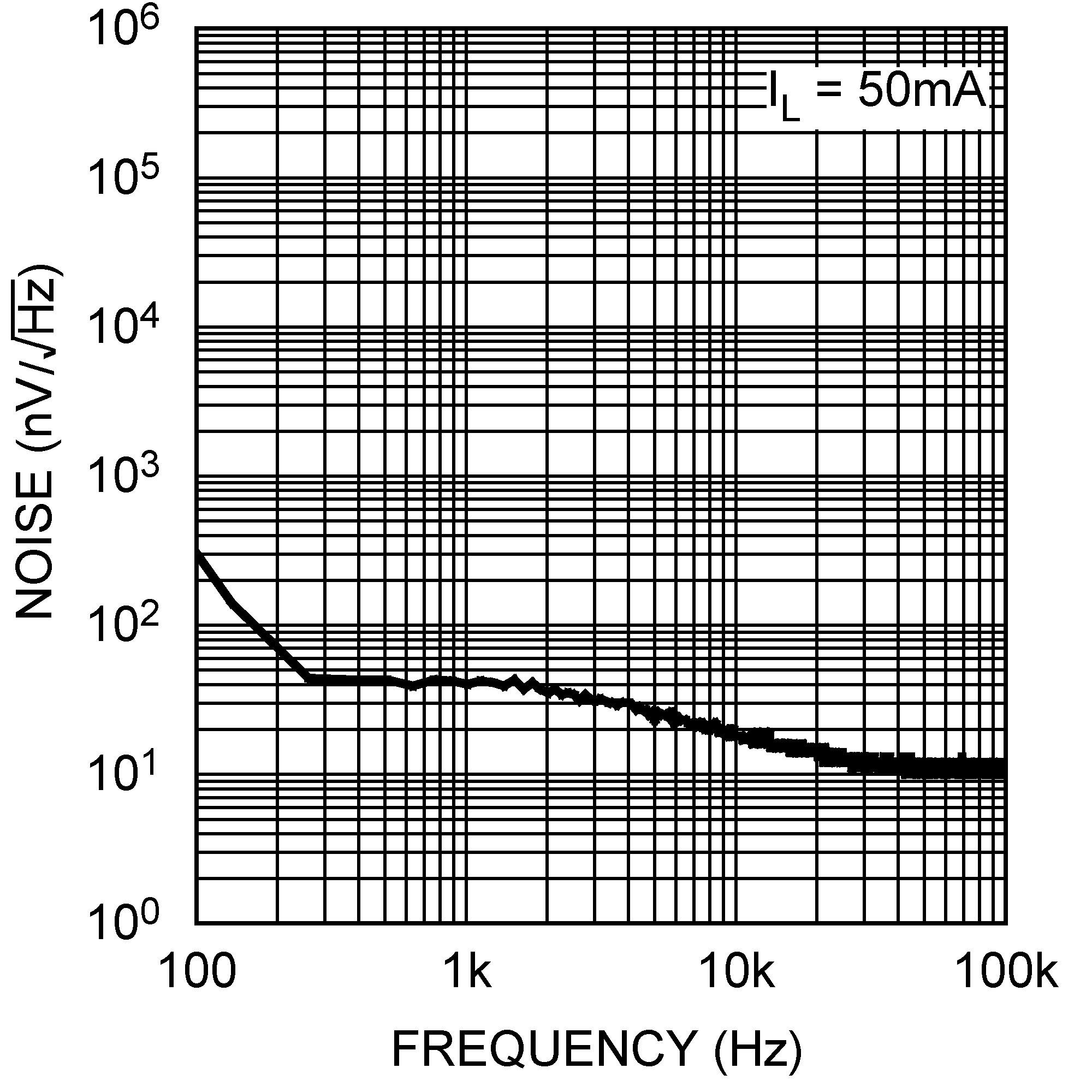 Figure 1. Output Noise Density
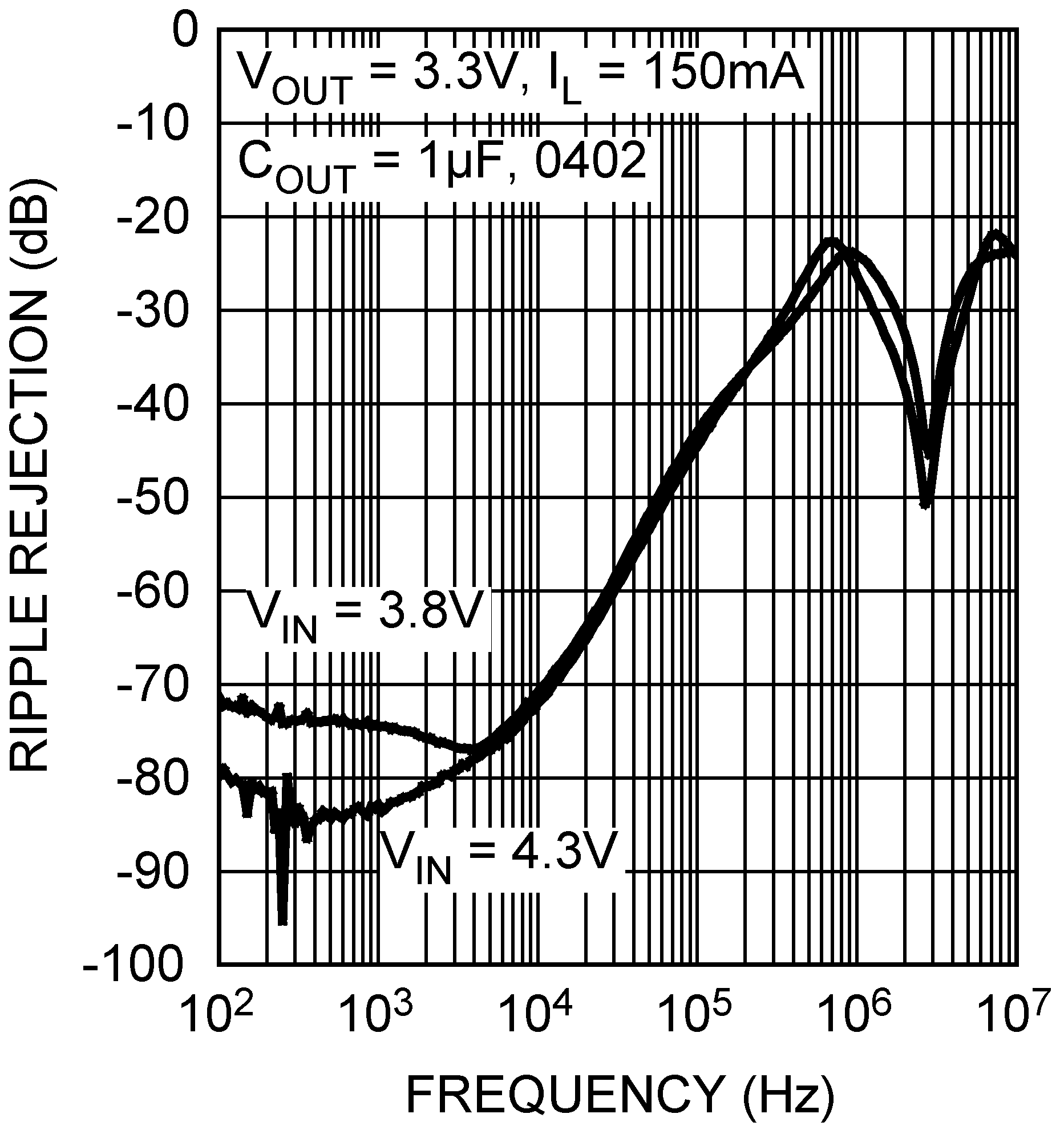 Figure 3. Power Supply Rejection Ratio
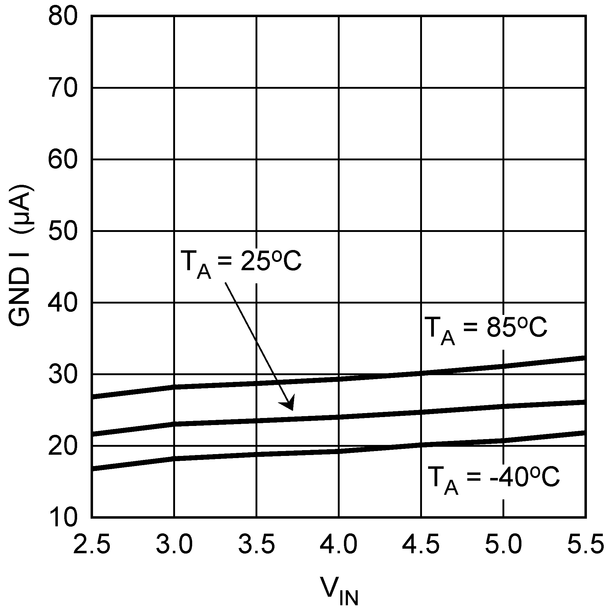 Figure 5. Ground Current vs VIN, I LOAD = 0 mA
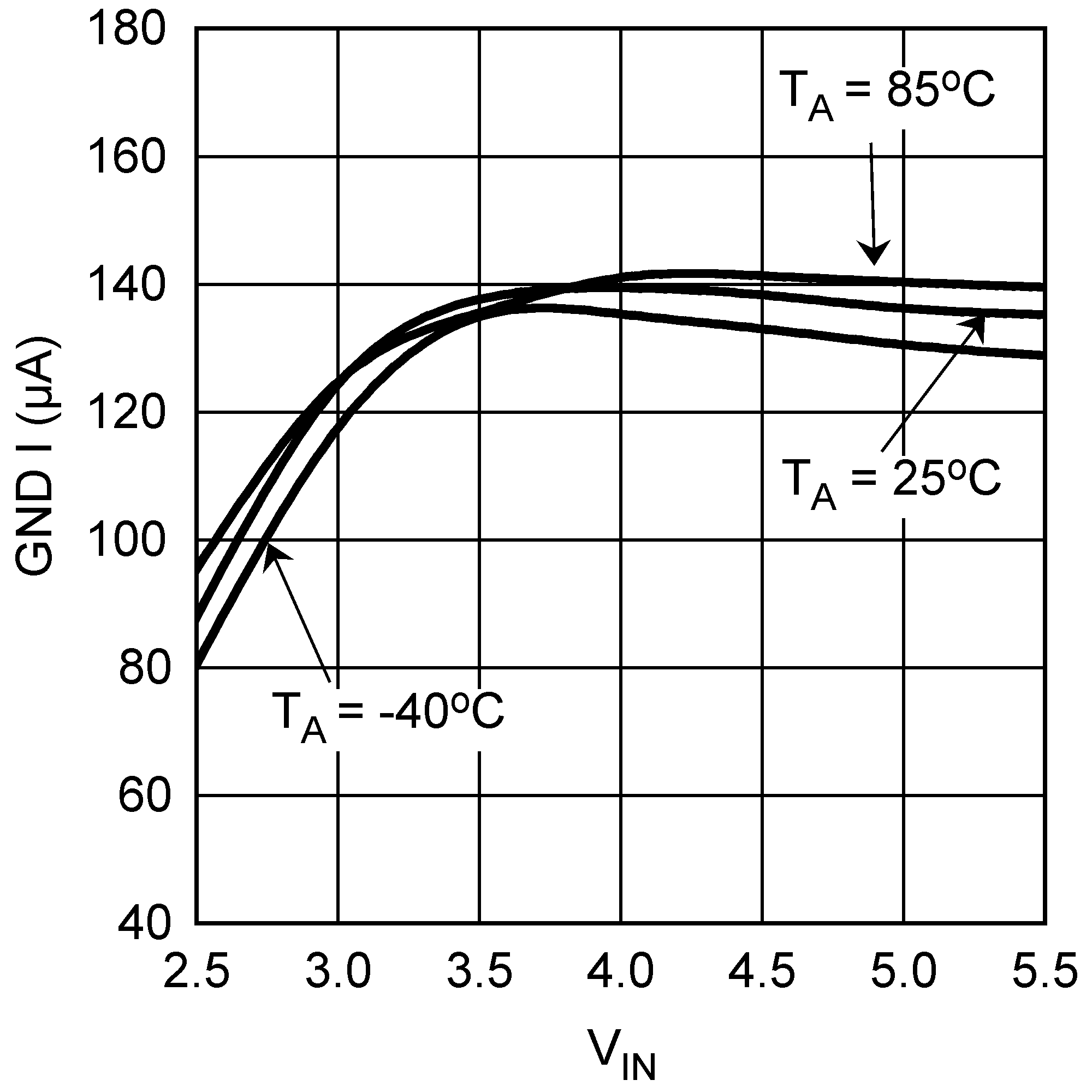 Figure 7. Ground Current vs VIN, I LOAD = 100 mA
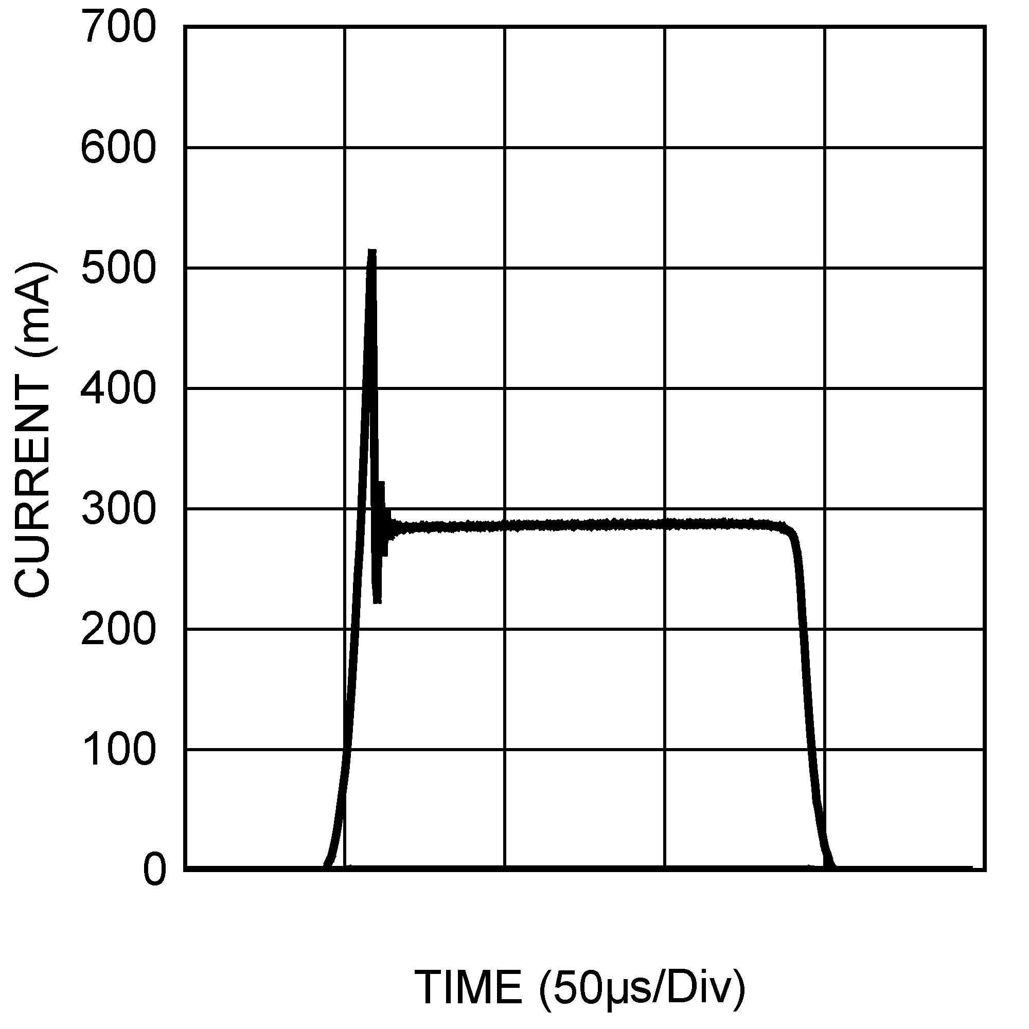 Figure 9. Short-Circuit Current
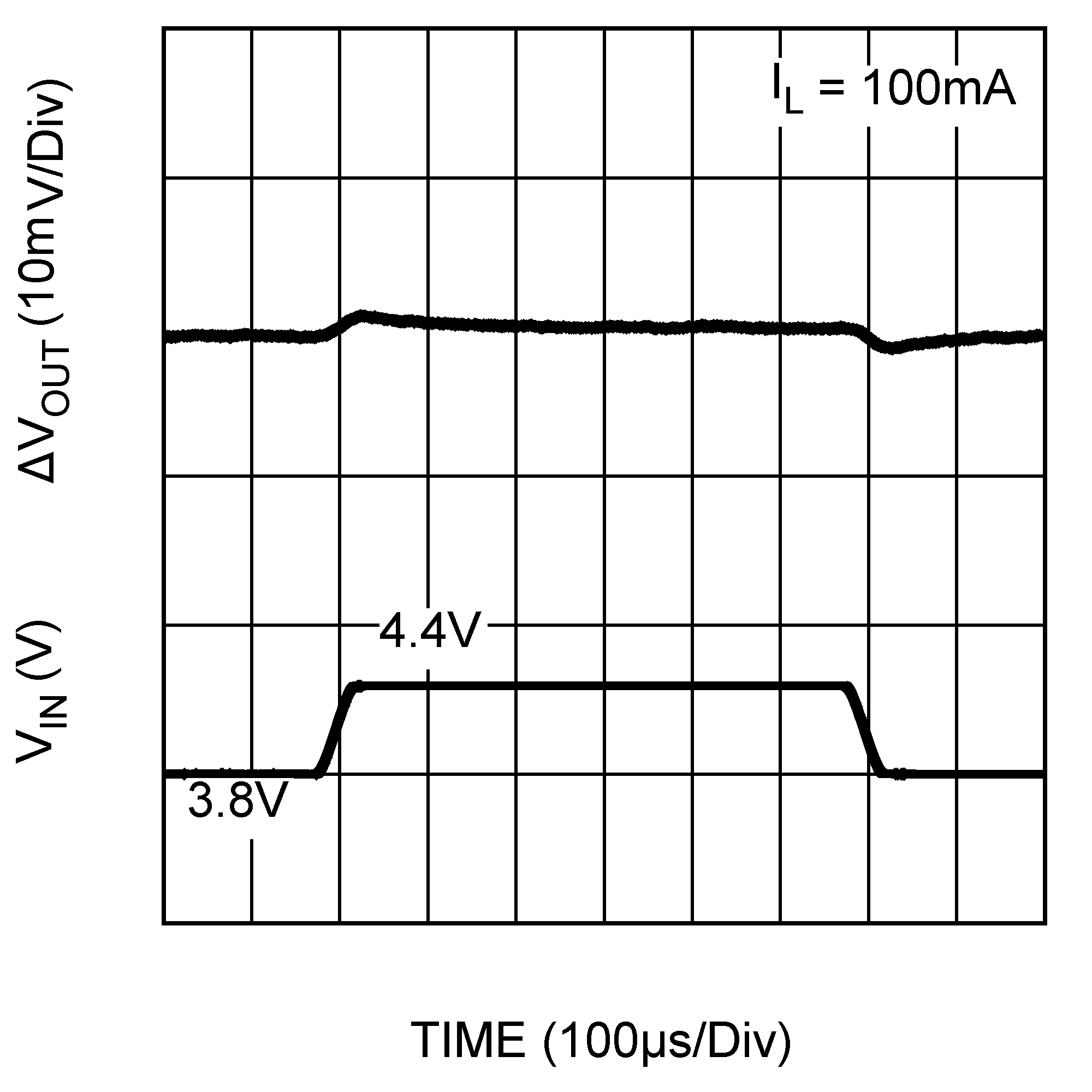 Figure 11. Line Transient
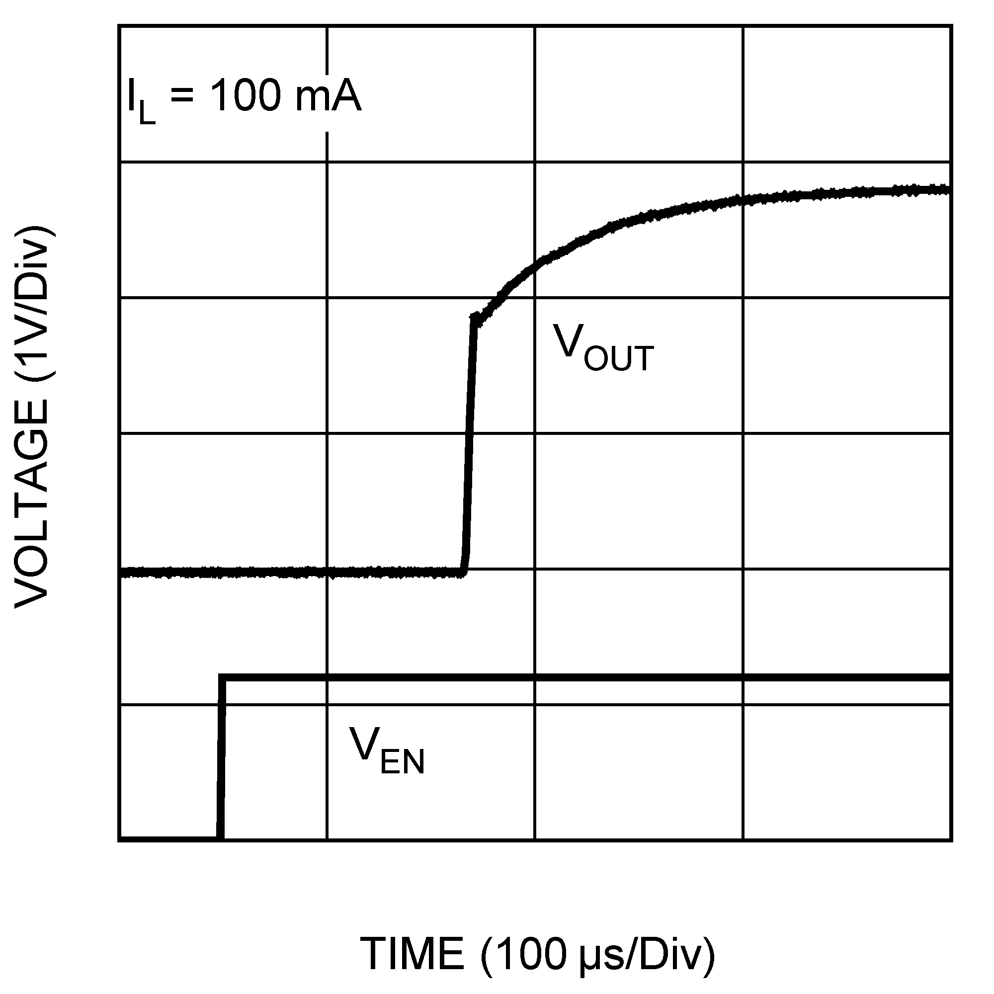 Figure 13. Enable Start-up Time, (IOUT= 100 mA, VOUT = 2.8 V)
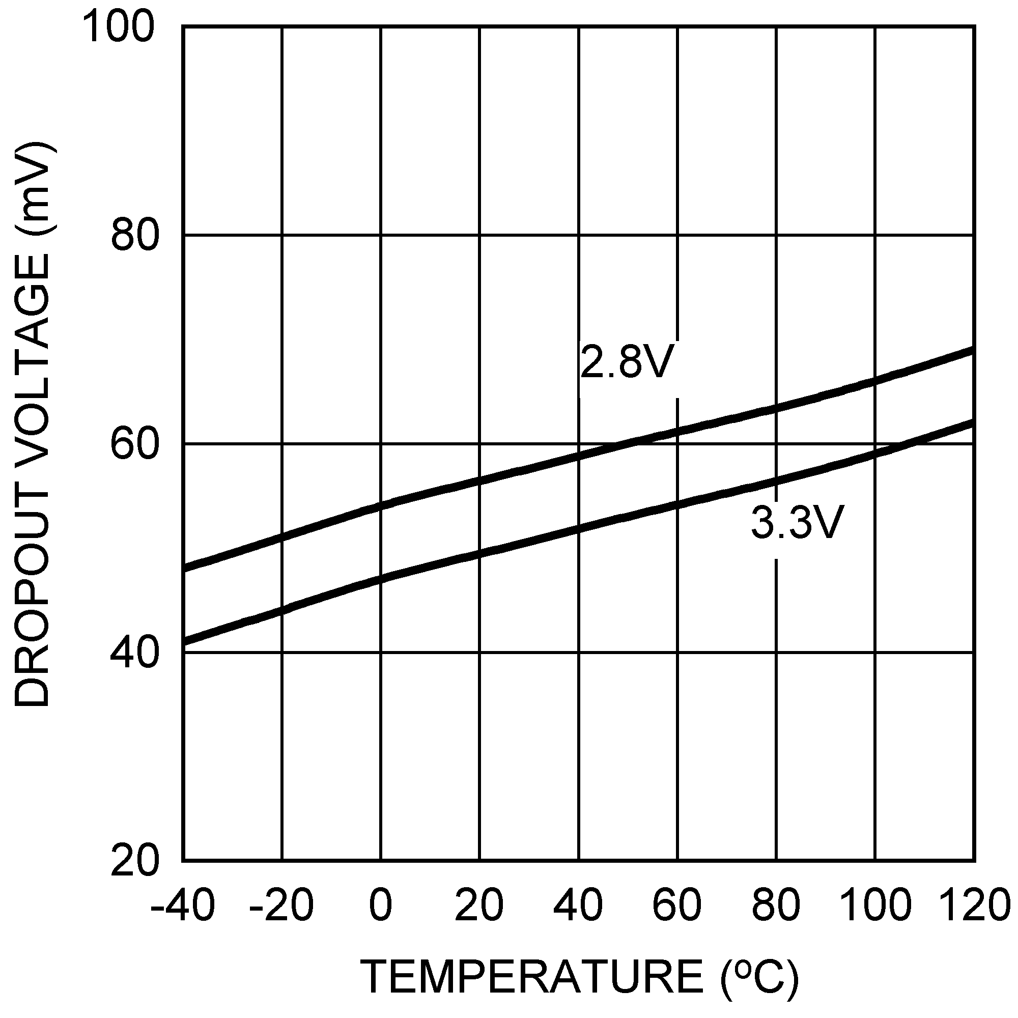 Figure 15. Dropout Over Temperature (100 mA)
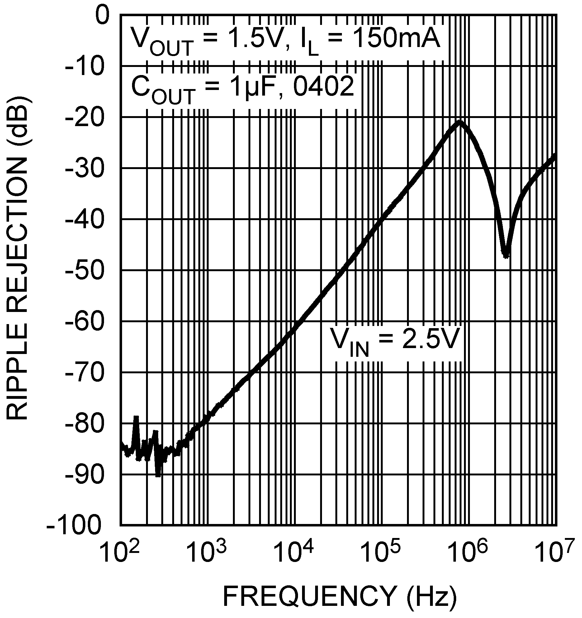 Figure 2. Power Supply Rejection Ratio
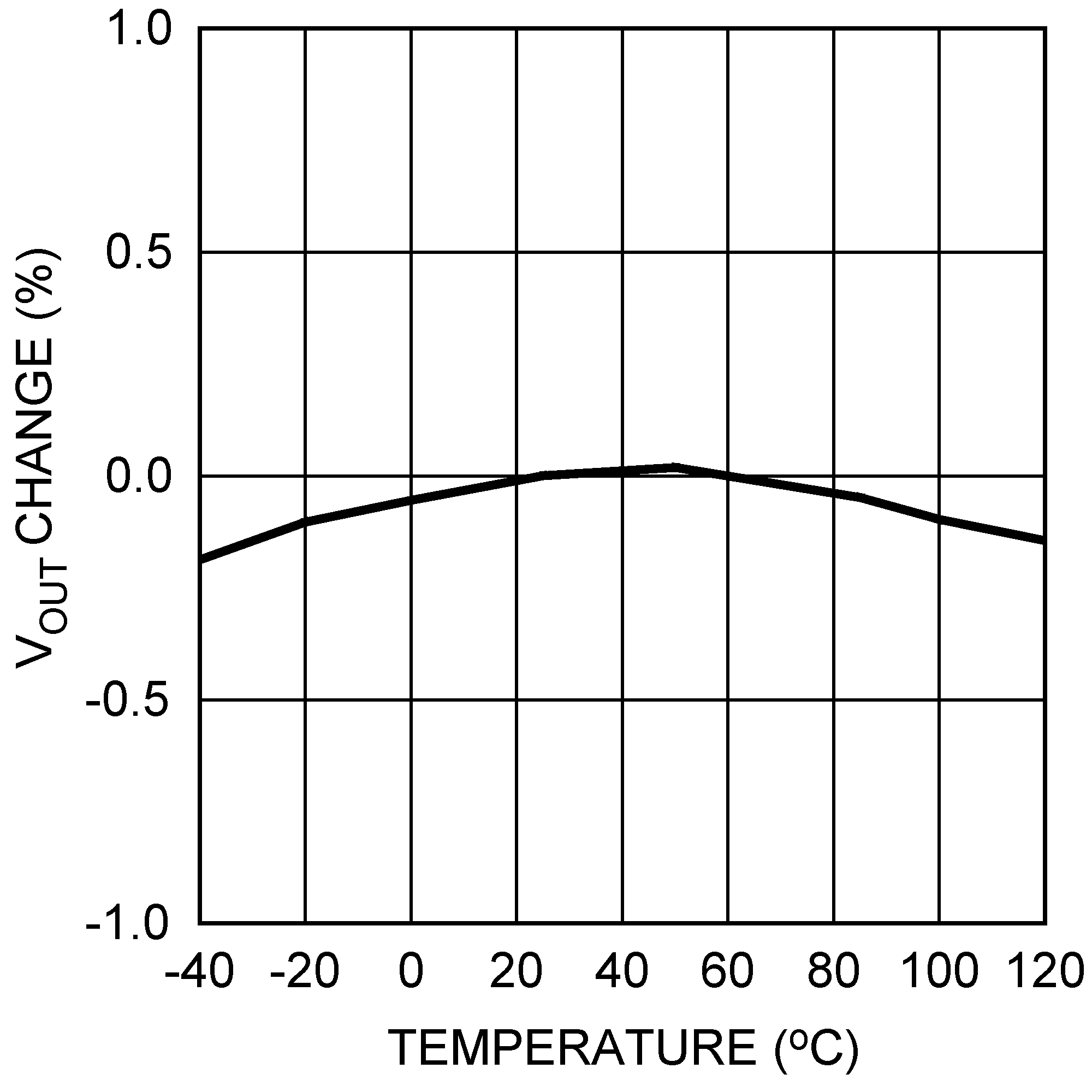 Figure 4. Output Voltage Change vs Temperature
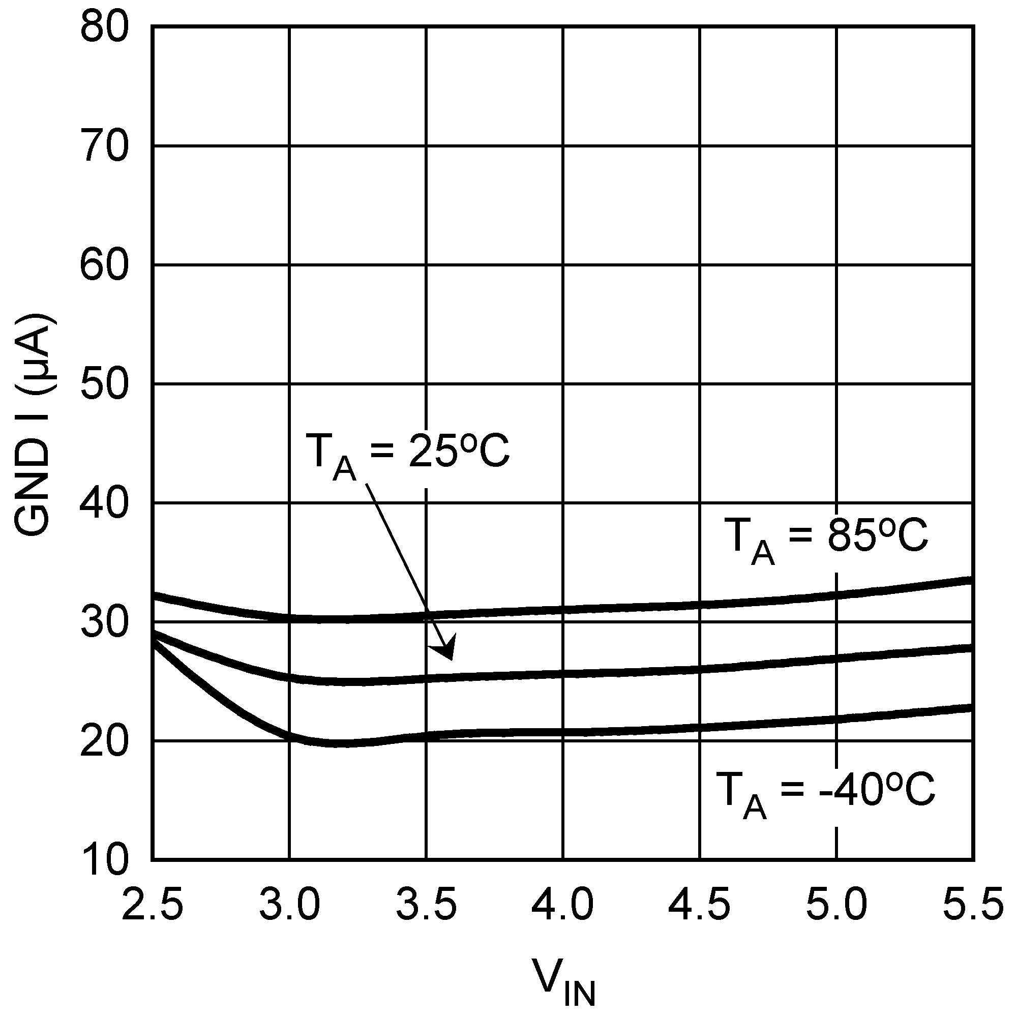 Figure 6. Ground Current vs VIN, I LOAD = 1 mA
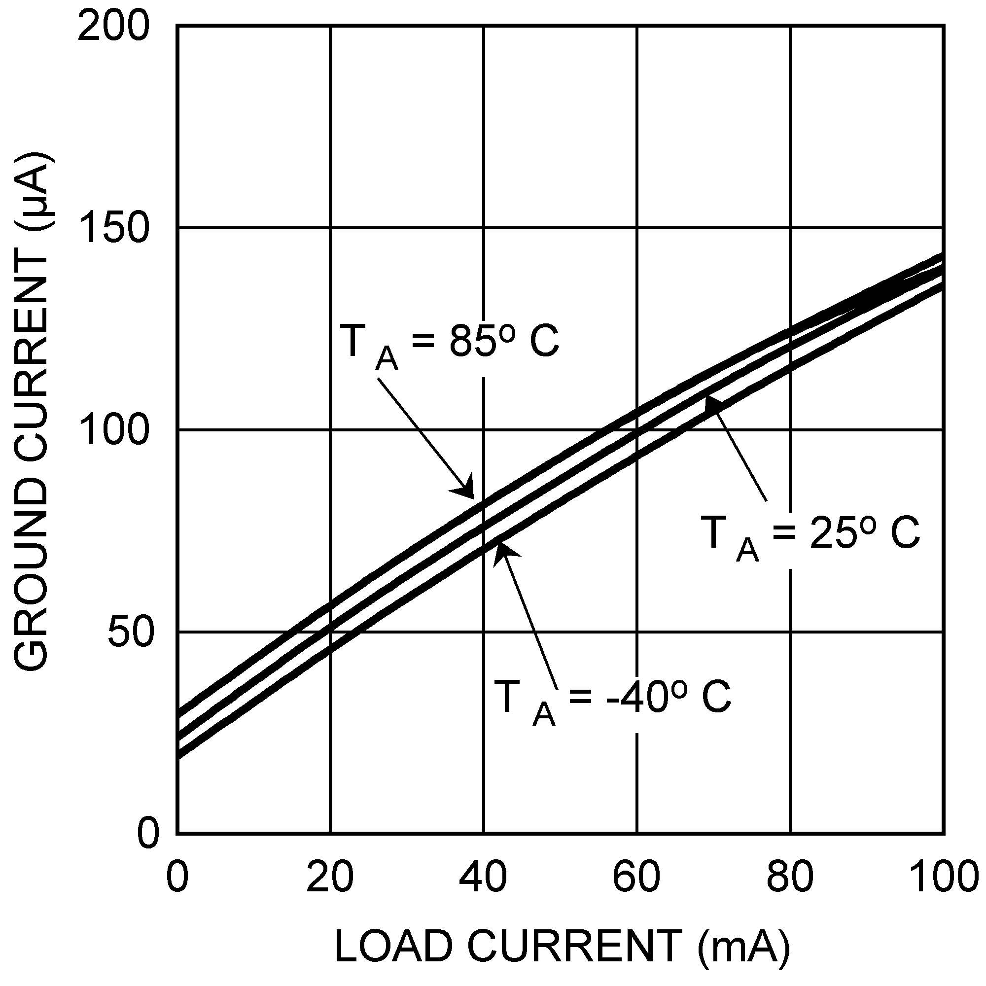 Figure 8. Ground Current vs Load Current
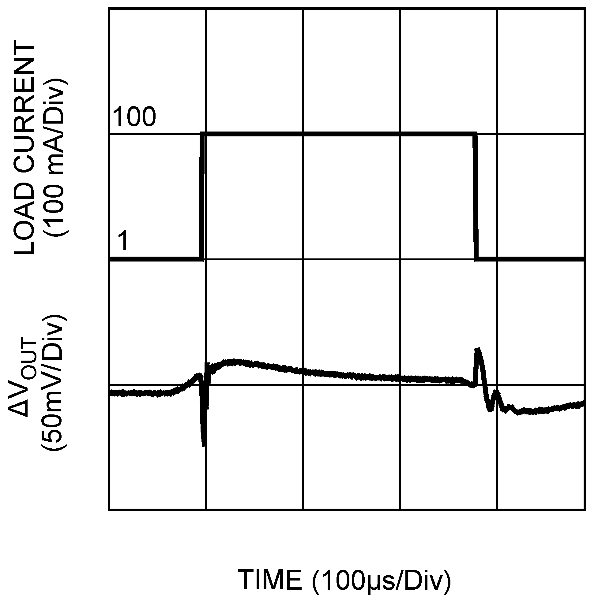 Figure 10. Load Transient
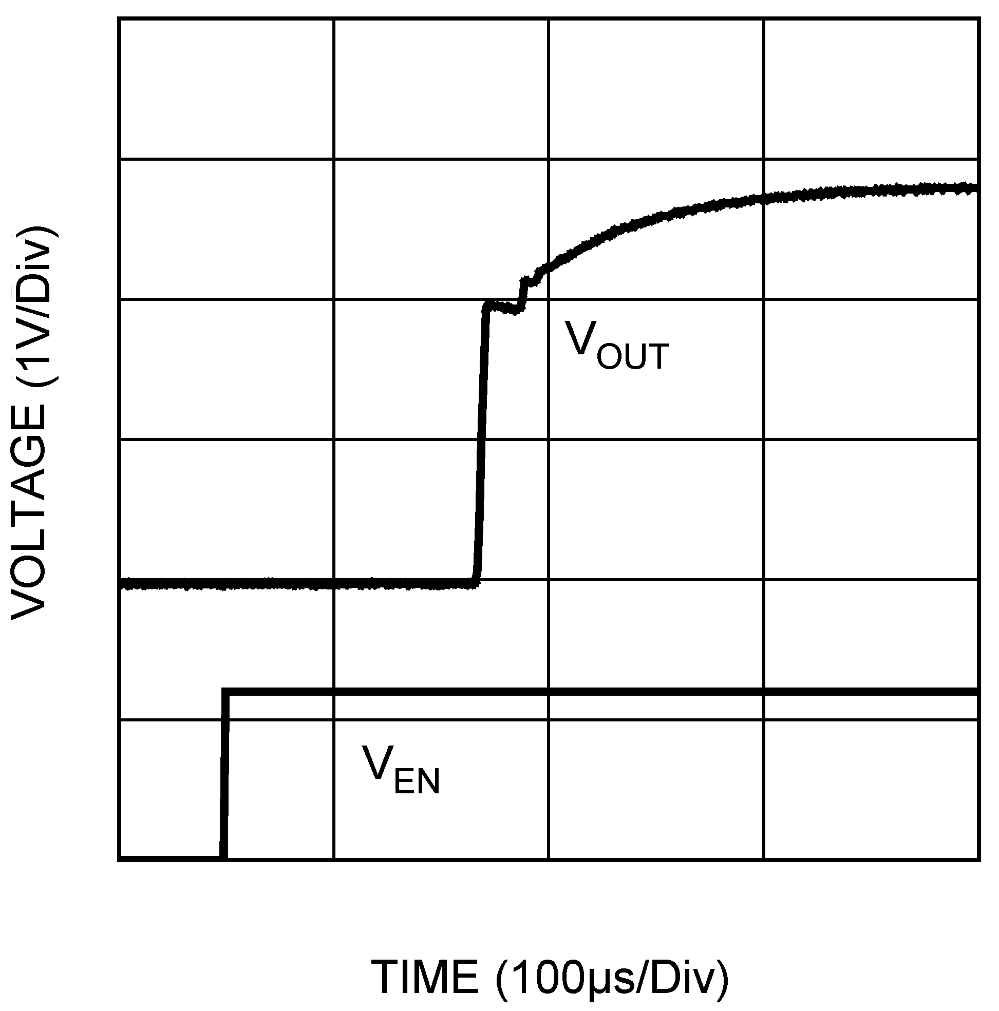 Figure 12. Enable Start-up Time, (IOUT= 1 mA, VOUT = 2.8 V)
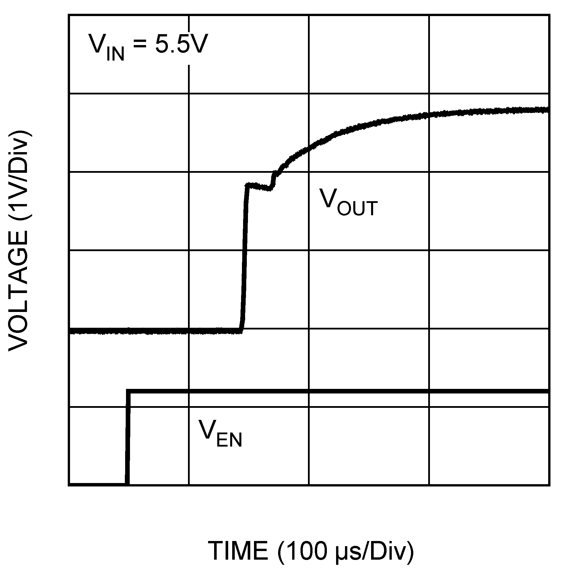 Figure 14. Enable Start-up Time, (IOUT= 1 mA, VOUT = 2.8 V)