ZHCSEY5D December 2015 – November 2016 LP5912
PRODUCTION DATA.
- 1 特性
- 2 应用
- 3 说明
- 4 修订历史记录
- 5 Voltage Options
- 6 Pin Configuration and Functions
- 7 Specifications
- 8 Detailed Description
- 9 Applications and Implementation
- 10Power Supply Recommendations
- 11Layout
- 12器件和文档支持
- 13机械、封装和可订购信息
9 Applications and Implementation
NOTE
Information in the following applications sections is not part of the TI component specification, and TI does not warrant its accuracy or completeness. TI’s customers are responsible for determining suitability of components for their purposes. Customers must validate and test their design implementation to confirm system functionality.
9.1 Application Information
The LP5912 is designed to meet the requirements of RF and analog circuits, by providing low noise, high PSRR, low quiescent current, and low line or load transient response. The device offers excellent noise performance without the need for a noise bypass capacitor and is stable with input and output capacitors with a value of 1 μF. The device delivers this performance in an industry standard WSON package, which for this device is specified with an operating junction temperature (TJ) of –40°C to +125°C.
9.2 Typical Application
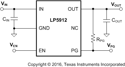
Figure 54 shows the typical application circuit for the LP5912. Input and output capacitances may need to be increased above the 1-μF minimum for some applications.
 Figure 54. LP5912 Typical Application
9.2.1 Design Requirements
For typical RF linear regulator applications, use the parameters listed in Table 1.
Table 1. Design Parameters
| DESIGN PARAMETER | EXAMPLE VALUE |
|---|---|
| Input voltage | 1.6 to 6.5 V |
| Output voltage | 0.8 to 5.5 V |
| Output current | 500 mA |
| Output capacitor | 1 to 10 µF |
| Input/output capacitor ESR range | 5 mΩ to 500 mΩ |
9.2.2 Detailed Design Procedure
9.2.2.1 External Capacitors
Like most low-dropout regulators, the LP5912 requires external capacitors for regulator stability. The device is specifically designed for portable applications requiring minimum board space and smallest components. These capacitors must be correctly selected for good performance.
9.2.2.2 Input Capacitor
An input capacitor is required for stability. The input capacitor must be at least equal to, or greater than, the output capacitor for good load-transient performance. A capacitor of at least 1 µF must be connected between the LP5912 IN pin and ground for stable operation over full load-current range. It is acceptable to have more output capacitance than input, as long as the input is at least 1 µF.
The input capacitor must be located a distance of not more than 1 cm from the input pin and returned to a clean analog ground. Any good-quality ceramic, tantalum, or film capacitor may be used at the input.
NOTE
To ensure stable operation it is essential that good PCB practices are employed to minimize ground impedance and keep input inductance low. If these conditions cannot be met, or if long leads are to be used to connect the battery or other power source to the LP5912, increasing the value of the input capacitor to at least 10 µF is recommended. Also, tantalum capacitors can suffer catastrophic failures due to surge current when connected to a low-impedance source of power (such as a battery or a very large capacitor). If a tantalum capacitor is used at the input, it must be verified by the manufacturer to have a surge current rating sufficient for the application. There are no requirements for the equivalent series resistance (ESR) on the input capacitor, but tolerance and temperature coefficient must be considered when selecting the capacitor to ensure the capacitance remains 1 μF ±30% over the entire operating temperature range.
9.2.2.3 Output Capacitor
The LP5912 is designed specifically to work with a very small ceramic output capacitor, typically 1 µF. A ceramic capacitor (dielectric types X5R or X7R) in the 1-µF to 10-µF range, and with an ESR from 5 mΩ to 500 mΩ, is suitable in the LP5912 application circuit. For this device the output capacitor must be connected between the OUT pin with a good connection back to the GND pin.
Tantalum or film capacitors may also be used at the device output, VOUT, but these are not as attractive for reasons of size and cost (see Capacitor Characteristics).
The output capacitor must meet the requirement for the minimum value of capacitance and have an ESR value that is within the range 5 mΩ to 500 mΩ for stability.
9.2.2.4 Capacitor Characteristics
The LP5912 is designed to work with ceramic capacitors on the input and output to take advantage of the benefits they offer. For capacitance values in the range of 1 µF to 10 µF, ceramic capacitors are the smallest, least expensive, and have the lowest ESR values, thus making them best for eliminating high frequency noise. The ESR of a typical 1-µF ceramic capacitor is in the range of 20 mΩ to 40 mΩ, which easily meets the ESR requirement for stability for the LP5912.
The preferred choice for temperature coefficient in a ceramic capacitor is X7R. This type of capacitor is the most stable and holds the capacitance within ±15% over the temperature range. Tantalum capacitors are less desirable than ceramic for use as output capacitors because they are more expensive when comparing equivalent capacitance and voltage ratings in the 1-µF to 10-µF range.
Another important consideration is that tantalum capacitors have higher ESR values than equivalent size ceramics. While it may be possible to find a tantalum capacitor with an ESR value within the stable range, it would have to be larger in capacitance (which means bigger and more costly) than a ceramic capacitor with the same ESR value. Also, the ESR of a typical tantalum increases about 2:1 as the temperature goes from 25°C down to –40°C, so some guard band must be allowed.
9.2.2.5 Remote Capacitor Operation
To ensure stability the LP5912 requires at least a 1-μF capacitor at the OUT pin. There is no strict requirement about the location of the output capacitor in regards to the LDO OUT pin; the output capacitor may be located 5 to 10 cm away from the LDO. This means that there is no need to have a special capacitor close to the OUT pin if there are already respective capacitors in the system. This placement flexibility requires that the output capacitor be connected directly between the LP5912 OUT pin and GND pin with no vias. This remote capacitor feature can help users to minimize the number of capacitors in the system.
As a good design practice, keep the wiring parasitic inductance at a minimum, which means using as wide as possible traces from the LDO output to the capacitors, keeping the LDO output trace layer as close to ground layer as possible, avoiding vias on the path. If there is a need to use vias, implement as many as possible vias between the connection layers. Keeping parasitic wiring inductance less than 35 nH is recommended. For applications with fast load transients use an input capacitor equal to, or larger than, the sum of the capacitance at the output node for the best load-transient performance.
9.2.2.6 Power Dissipation
Knowing the device power dissipation and proper sizing of the thermal plane connected to the tab or pad is critical to ensuring reliable operation. Device power dissipation depends on input voltage, output voltage, and load conditions and can be calculated with Equation 1.
Power dissipation can be minimized, and greater efficiency can be achieved, by using the lowest available voltage drop option that is greater than the dropout voltage (VDO). However, keep in mind that higher voltage drops result in better dynamic (that is, PSRR and transient) performance.
On the WSON (DRV) package, the primary conduction path for heat is through the exposed power pad into the PCB. To ensure the device does not overheat, connect the exposed pad, through thermal vias, to an internal ground plane with an appropriate amount of copper PCB area.
Power dissipation and junction temperature are most often related by the junction-to-ambient thermal resistance (RθJA) of the combined PCB and device package and the temperature of the ambient air (TA), according to Equation 2 or Equation 3:
Unfortunately, this RθJA is highly dependent on the heat-spreading capability of the particular PCB design, and therefore varies according to the total copper area, copper weight, and location of the planes. The RθJA recorded in Thermal Information is determined by the specific EIA/JEDEC JESD51-7 standard for PCB and copper-spreading area, and is to be used only as a relative measure of package thermal performance. For a well-designed thermal layout, RθJA is actually the sum of the package junction-to-case (bottom) thermal resistance (RθJCbot) plus the thermal resistance contribution by the PCB copper area acting as a heat sink.
9.2.2.7 Estimating Junction Temperature
The EIA/JEDEC standard recommends the use of psi (Ψ) thermal characteristics to estimate the junction temperatures of surface mount devices on a typical PCB board application. These characteristics are not true thermal resistance values, but rather package specific thermal characteristics that offer practical and relative means of estimating junction temperatures. These psi metrics are determined to be significantly independent of copper-spreading area. The key thermal characteristics (ΨJT and ΨJB) are given in Thermal Information and are used in accordance with Equation 4 or Equation 5.
where
- PD(MAX) is explained in Equation 3
- TTOP is the temperature measured at the center-top of the device package.
where
- PD(MAX) is explained in Equation 3.
- TBOARD is the PCB surface temperature measured 1 mm from the device package and centered on the package edge.
For more information about the thermal characteristics ΨJT and ΨJB, see Semiconductor and IC Package Thermal Metrics ; for more information about measuring TTOP and TBOARD, see Using New Thermal Metrics ; and for more information about the EIA/JEDEC JESD51 PCB used for validating RθJA, see the TI Application Report Thermal Characteristics of Linear and Logic Packages Using JEDEC PCB Designs. These application notes are available at www.ti.com.
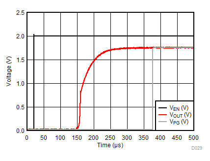
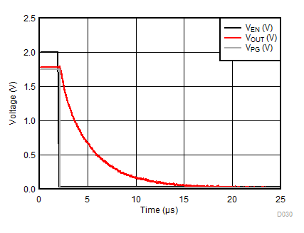
9.2.3 Application Curves

| VIN = 2.3 V | IOUT = 500 mA | COUT = 1 µF |

| VIN = 2.3 V | IOUT = 500 mA (3.6 Ω) | COUT = 1 µF |