ZHCSFR8 November 2016 LP5922
PRODUCTION DATA.
- 1 特性
- 2 应用
- 3 说明
- 4 修订历史记录
- 5 Pin Configuration and Functions
- 6 Specifications
- 7 Detailed Description
-
8 Applications and Implementation
- 8.1 Application Information
- 8.2
Typical Application
- 8.2.1 Design Requirements
- 8.2.2
Detailed Design Procedure
- 8.2.2.1 External Capacitors
- 8.2.2.2 Input Capacitor, CIN
- 8.2.2.3 Output Capacitor, COUT
- 8.2.2.4 Soft-Start and Noise-Reduction Capacitor, CSS/NR
- 8.2.2.5 Feed-Forward Capacitor, CFF
- 8.2.2.6 No-Load Stability
- 8.2.2.7 Power Dissipation
- 8.2.2.8 Estimating Junction Temperature
- 8.2.2.9 Recommended Continuous Operating Area
- 8.2.3 Application Curves
- 9 Power Supply Recommendations
- 10Layout
- 11器件和文档支持
- 12机械、封装和可订购信息
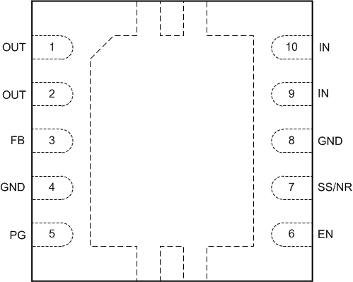
5 Pin Configuration and Functions
DSC Package
10-Pin WSON With Thermal Pad
Top View

Pin Functions
| PIN | I/O | DESCRIPTION | |
|---|---|---|---|
| NUMBER | NAME | ||
| 1 | OUT | O | Regulated output voltage, connect directly to pin 2 |
| 2 | OUT | O | Regulated output voltage, connect directly to pin 1 |
| 3 | FB | I | Voltage feedback input to the internal error amplifier |
| 4 | GND | Ground | Ground; connect to device pin 8. |
| 5 | PG | O | Power Good to indicate the status of output voltage. Requires an external pull-up resistor. When PG pin voltage is high the output voltage is considered good. |
| 6 | EN | I | Enable |
| 7 | SS/NR | I/O | Soft-start and noise reduction pin |
| 8 | GND | Ground | Ground —connect to device pin 4. |
| 9 | IN | I | Supply voltage input — connect directly to pin 10. |
| 10 | IN | I | Supply voltage input —connect directly to pin 9. |
| Exposed pad | Thermal Pad | — | The exposed thermal pad on the bottom of the package must be connected to a copper area under the package on the PCB. Connect to ground potential. Do not connect to any potential other than the same ground potential seen at device pins 4 and 8 (GND). See Power Dissipation for more information. |