ZHCSD61L July   2012  – May 2019 LP8556

PRODUCTION DATA.  

  1. 特性
  2. 应用
    1.     简化原理图
  3. 说明
  4. 修订历史记录
  5. Device Options
  6. Pin Configuration and Functions
    1.     Pin Functions
  7. Specifications
    1. 7.1  Absolute Maximum Ratings
    2. 7.2  ESD Ratings
    3. 7.3  Recommended Operating Conditions
    4. 7.4  Thermal Information
    5. 7.5  Electrical Characteristics
    6. 7.6  Electrical Characteristics — Boost Converter
    7. 7.7  Electrical Characteristics — LED Driver
    8. 7.8  Electrical Characteristics — PWM Interface
    9. 7.9  Electrical Characteristics — Logic Interface
    10. 7.10 I2C Serial Bus Timing Parameters (SDA, SCL)
    11. 7.11 Typical Characteristics
  8. Detailed Description
    1. 8.1 Overview
    2. 8.2 Functional Block Diagram
    3. 8.3 Feature Description
      1. 8.3.1 Boost Converter
        1. 8.3.1.1 Boost Converter Operation
        2. 8.3.1.2 Setting Boost Switching Frequency
        3. 8.3.1.3 Output Voltage Control
          1. 8.3.1.3.1 Adaptive Control
          2. 8.3.1.3.2 Manual Control
        4. 8.3.1.4 EMI Reduction
      2. 8.3.2 Brightness Control
        1. 8.3.2.1  BRT_MODE = 00
        2. 8.3.2.2  BRT_MODE = 01
        3. 8.3.2.3  BRT_MODE = 10
        4. 8.3.2.4  BRT_MODE = 11
        5. 8.3.2.5  Output Dimming Schemes
          1. 8.3.2.5.1 PWM Control
          2. 8.3.2.5.2 Pure Current Control
          3. 8.3.2.5.3 Adaptive Control
        6. 8.3.2.6  Setting Full-Scale LED Current
        7. 8.3.2.7  Setting PWM Dimming Frequency
        8. 8.3.2.8  Phase Shift PWM Scheme
        9. 8.3.2.9  Slope and Advanced Slope
        10. 8.3.2.10 Dithering
      3. 8.3.3 Fault Detection
        1. 8.3.3.1 LED Fault Detection
          1. 8.3.3.1.1 Open Detect
          2. 8.3.3.1.2 Short Detect
        2. 8.3.3.2 Undervoltage Detection
        3. 8.3.3.3 Overcurrent Protection
        4. 8.3.3.4 Thermal Shutdown
    4. 8.4 Device Functional Modes
      1. 8.4.1 Shutdown Mode
      2. 8.4.2 Active Mode
    5. 8.5 Programming
      1. 8.5.1 I2C-Compatible Serial Bus Interface
        1. 8.5.1.1 Interface Bus Overview
        2. 8.5.1.2 Data Transactions
        3. 8.5.1.3 Acknowledge Cycle
        4. 8.5.1.4 Acknowledge After Every Byte Rule
        5. 8.5.1.5 Addressing Transfer Formats
        6. 8.5.1.6 Control Register Write Cycle
        7. 8.5.1.7 Control Register Read Cycle
        8. 8.5.1.8 Register Read and Write Detail
    6. 8.6 Register Maps
      1. 8.6.1 Register Bit Explanations
        1. 8.6.1.1 Brightness Control
        2. 8.6.1.2 Device Control
        3. 8.6.1.3 Status
        4. 8.6.1.4 Direct Control
        5. 8.6.1.5 LED String Enable
      2. 8.6.2 EPROM Bit Explanations
        1. 8.6.2.1  LP8556TM (DSBGA) Configurations and Pre-Configured EPROM Settings
        2. 8.6.2.2  LP8556TM (DSBGA) Configurations and Pre-configured EPROM Settings Continued
        3. 8.6.2.3  LP8556SQ (WQFN) Configurations and Pre-configured EPROM Settings
        4. 8.6.2.4  CFG98
        5. 8.6.2.5  CFG9E
        6. 8.6.2.6  CFG0
        7. 8.6.2.7  CFG1
        8. 8.6.2.8  CFG2
        9. 8.6.2.9  CFG3
        10. 8.6.2.10 CFG4
        11. 8.6.2.11 CFG5
        12. 8.6.2.12 CFG6
        13. 8.6.2.13 CFG7
        14. 8.6.2.14 CFG9
        15. 8.6.2.15 CFGA
        16. 8.6.2.16 CFGE
        17. 8.6.2.17 CFGF
  9. Application and Implementation
    1. 9.1 Application Information
      1. 9.1.1 Using LP8556 With I2C Host
        1. 9.1.1.1 Setting Boost Switching and PWM Dimming Frequencies
        2. 9.1.1.2 Setting Full-Scale LED Current
      2. 9.1.2 Using LP8556 With Configuration Resistors and IO Pins
        1. 9.1.2.1 Setting Boost Switching and PWM Dimming Frequencies
        2. 9.1.2.2 Setting Full-Scale LED Current
    2. 9.2 Typical Application
      1. 9.2.1 Design Requirements
      2. 9.2.2 Detailed Design Procedure
        1. 9.2.2.1 Recommended Inductance for the Boost Power Stage
        2. 9.2.2.2 Recommended Capacitances for the Boost and LDO Power Stages
      3. 9.2.3 Application Curves
  10. 10Power Supply Recommendations
  11. 11Layout
    1. 11.1 Layout Guidelines
    2. 11.2 Layout Examples
  12. 12器件和文档支持
    1. 12.1 接收文档更新通知
    2. 12.2 社区资源
    3. 12.3 商标
    4. 12.4 静电放电警告
    5. 12.5 Glossary
  13. 13机械、封装和可订购信息

封装选项

机械数据 (封装 | 引脚)
散热焊盘机械数据 (封装 | 引脚)
订购信息

Application Curves

Unless otherwise specified: VIN = 3.8 V, CVLDO = 10 μF, L1 = 4.7 μH, CIN = 2.2 μF, COUT = 4.7 μF, ƒSW = 1.25 MHz
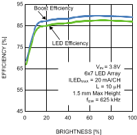
LP8556 30162652.gifFigure 20. Boost and LED Drive Efficiency
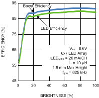
LP8556 30162654.gifFigure 22. Boost and LED Drive Efficiency
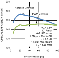
LP8556 30162656.gifFigure 24. Optical Efficiency
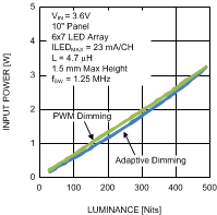
LP8556 30162658.gifFigure 26. Input Power as a Function of Brightness
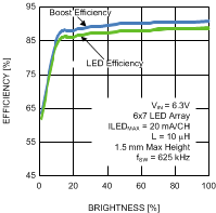
LP8556 30162653.gifFigure 21. Boost and LED Drive Efficiency
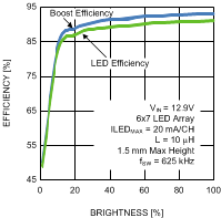
LP8556 30162655.gifFigure 23. Boost and LED Drive Efficiency
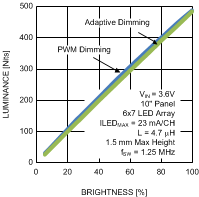
LP8556 30162657.gifFigure 25. Luminance as a Function of Brightness
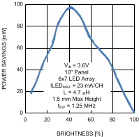
LP8556 30162659.gifFigure 27. Power Savings With Adaptive Dimming when Compared to PWM Dimming