ZHCSD61L July 2012 – May 2019 LP8556
PRODUCTION DATA.
- 1 特性
- 2 应用
- 3 说明
- 4 修订历史记录
- 5 Device Options
- 6 Pin Configuration and Functions
-
7 Specifications
- 7.1 Absolute Maximum Ratings
- 7.2 ESD Ratings
- 7.3 Recommended Operating Conditions
- 7.4 Thermal Information
- 7.5 Electrical Characteristics
- 7.6 Electrical Characteristics — Boost Converter
- 7.7 Electrical Characteristics — LED Driver
- 7.8 Electrical Characteristics — PWM Interface
- 7.9 Electrical Characteristics — Logic Interface
- 7.10 I2C Serial Bus Timing Parameters (SDA, SCL)
- 7.11 Typical Characteristics
-
8 Detailed Description
- 8.1 Overview
- 8.2 Functional Block Diagram
- 8.3
Feature Description
- 8.3.1 Boost Converter
- 8.3.2 Brightness Control
- 8.3.3 Fault Detection
- 8.4 Device Functional Modes
- 8.5 Programming
- 8.6
Register Maps
- 8.6.1 Register Bit Explanations
- 8.6.2
EPROM Bit Explanations
- 8.6.2.1 LP8556TM (DSBGA) Configurations and Pre-Configured EPROM Settings
- 8.6.2.2 LP8556TM (DSBGA) Configurations and Pre-configured EPROM Settings Continued
- 8.6.2.3 LP8556SQ (WQFN) Configurations and Pre-configured EPROM Settings
- 8.6.2.4 CFG98
- 8.6.2.5 CFG9E
- 8.6.2.6 CFG0
- 8.6.2.7 CFG1
- 8.6.2.8 CFG2
- 8.6.2.9 CFG3
- 8.6.2.10 CFG4
- 8.6.2.11 CFG5
- 8.6.2.12 CFG6
- 8.6.2.13 CFG7
- 8.6.2.14 CFG9
- 8.6.2.15 CFGA
- 8.6.2.16 CFGE
- 8.6.2.17 CFGF
- 9 Application and Implementation
- 10Power Supply Recommendations
- 11Layout
- 12器件和文档支持
- 13机械、封装和可订购信息
封装选项
机械数据 (封装 | 引脚)
散热焊盘机械数据 (封装 | 引脚)
- RTW|24
订购信息
6 Pin Configuration and Functions
YFQ Package
20-Pin DSBGA
Top View

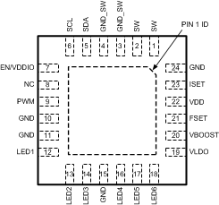
RTW Package
24-Pin WQFN
Top View

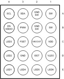
YFQ Package
20-Pin DSBGA
Bottom View

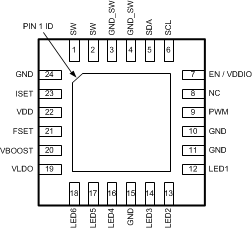
RTW Package
24-Pin WQFN
Bottom View

Pin Functions
| PIN | TYPE(1) | DESCRIPTION | ||
|---|---|---|---|---|
| DSBGA | WQFN | NAME | ||
| A1, B1 | 1, 2 | SW | A | A connection to the drain terminal of the integrated power MOSFET. |
| A2, B2 | 3, 4 | GND_SW | G | A connection to the source terminal of the integrated power MOSFET. |
| A3 | 5 | SDA | I/O | I2C data input/output pin |
| A4 | 6 | SCL | I | I2C clock input pin |
| B3 | 9 | PWM | I | PWM dimming input. Supply a 75-Hz to 25-kHz PWM signal to control dimming. This pin must be connected to GND if unused. |
| B4 | 7 | EN / VDDIO | P | Dual-purpose pin serving both as a chip enable and as a power supply reference for PWM, SDA, and SCL inputs. Drive this pin with a logic gate capable of sourcing a minimum of 1 mA. |
| C1 | 22 | VDD | P | Device power supply pin. Provide 2.7-V to 20-V supply to this pin. This pin is an input of the internal LDO regulator. The output of the internal LDO is what powers the device. |
| C2 | 20 | VBOOST | A | Boost converter output pin. The internal feedback (FB) and overvoltage protection (OVP) circuitry monitors the voltage on this pin. Connect the converter output capacitor bank close to this pin. |
| C3 | 21 | FSET | A | A connection for setting the boost frequency and PWM output dimming frequency by using an external resistor. Connect a resistor, RFSET, between this pin and the ground reference (see Table 5). This pin may be left floating if PWM_FSET_EN = 0 AND BOOST_FSET_EN = 0 (see Table 10). |
| C4 | 14 | LED3 | A | LED driver - current sink terminal. If unused, it may be left floating. |
| D1 | 19 | VLDO | P | Internal LDO output pin. Connect a capacitor, CVLDO, between this pin and the ground reference. |
| D2 | 23 | ISET | A | A connection for the LED current set resistor. Connect a resistor, RISET, between this pin and the ground reference. This pin may be left floating if ISET_EN = 0 (see Table 10). |
| D3 | 10, 11, 15, 24, DAP | GND | I | Ground pin. |
| D4 | 13 | LED2 | A | LED driver - current sink pin. If unused, it may be left floating. |
| E1 | 18 | LED6 | A | LED driver - current sink pin. If unused, it may be left floating. |
| E2 | 17 | LED5 | A | LED driver - current sink pin. If unused, it may be left floating. |
| E3 | 16 | LED4 | A | LED driver - current sink pin. If unused, it may be left floating. |
| E4 | 12 | LED1 | A | LED driver - current sink pin. If unused, it may be left floating. |
| — | 8 | NC | — | No Connect pin. |
(1) A: Analog Pin, G: Ground Pin, P: Power Pin, I: Digital Input Pin, I/O: Digital Input/Output Pin