SNVSA28 December 2014 LP8731-Q1
PRODUCTION DATA.
- 1 Features
- 2 Applications
- 3 Description
- 4 Revision History
- 5 Device Comparison Tables
- 6 Pin Configuration and Functions
-
7 Specifications
- 7.1 Absolute Maximum Ratings
- 7.2 ESD Ratings
- 7.3 Recommended Operating Conditions (Bucks)
- 7.4 Thermal Information
- 7.5 General Electrical Characteristics
- 7.6 Low Dropout Regulators, LDO1 And LDO2
- 7.7 Buck Converters SW1, SW2
- 7.8 I/O Electrical Characteristics
- 7.9 Power-On Reset Threshold/Function (POR)
- 7.10 I2C-Compatible Interface Timing
- 7.11 Typical Characteristics
-
8 Detailed Description
- 8.1 Overview
- 8.2 Functional Block Diagram
- 8.3
Features Description
- 8.3.1 Linear Low Dropout Regulators (LDOs)
- 8.3.2 No-Load Stability
- 8.3.3 LDO1 and LDO2 Control Registers
- 8.3.4
SW1, SW2: Synchronous Step-Down Magnetic DC-DC Converters
- 8.3.4.1 Functional Description
- 8.3.4.2 Circuit Operation
- 8.3.4.3 PWM Operation
- 8.3.4.4 Internal Synchronous Rectification
- 8.3.4.5 Current Limiting
- 8.3.4.6 SW1, SW2 Operation
- 8.3.4.7 SW1, SW2 Control Registers
- 8.3.4.8 Shutdown Mode
- 8.3.4.9 Soft Start
- 8.3.4.10 Low Dropout Operation
- 8.3.4.11 Flexible Power Sequencing of Multiple Power Supplies
- 8.3.4.12 Power-Up Sequencing Using the EN_T Function
- 8.3.5 Flexible Power-On Reset (for example, Power Good with Delay)
- 8.3.6 Undervoltage Lockout
- 8.4 Device Functional Modes
- 8.5 Programming
- 8.6
LP8731-Q1 Register Maps
- 8.6.1 Interrupt Status Register (ISRA) 0x02
- 8.6.2 System Control 1 Register (SCR1) 0x07
- 8.6.3 EN_DLY Preset Delay Sequence after EN_T Assertion
- 8.6.4 Buck and LDO Output Voltage Enable Register (BKLDOEN) - 0x10
- 8.6.5 Buck and LDO Status Register (BKLDOSR) - 0x11
- 8.6.6 BUCK Voltage Change Control Register 1 (VCCR) - 0x20
- 8.6.7 BUCK1 Target Voltage 1 Register (B1TV1) - 0x23
- 8.6.8 BUCK1 Target Voltage 2 Register (B1TV2) - 0x24
- 8.6.9 BUCK1 Ramp Control Register (B1RC) - 0x25
- 8.6.10 BUCK2 Target 1 Register (B2TV1) - 0x29
- 8.6.11 BUCK2 Target 2 Register (B2TV2) - 0x2A
- 8.6.12 BUCK2 Ramp Control Register (B2RC) - 0x2B
- 8.6.13 BUCK Function Register (BFCR) - 0x38
- 8.6.14 Spread Spectrum Function
- 8.6.15 LDO1 Control Register (LDO1VCR) - 0x39
- 8.6.16 LDO2 Control Register (LDO2VCR) - 0x3A
- 9 Application and Implementation
- 10Power Supply Recommendations
- 11Layout
- 12Device and Documentation Support
- 13Mechanical, Packaging, and Orderable Information
9 Application and Implementation
NOTE
Information in the following applications sections is not part of the TI component specification, and TI does not warrant its accuracy or completeness. TI’s customers are responsible for determining suitability of components for their purposes. Customers should validate and test their design implementation to confirm system functionality.
9.1 Application Information
One of the key features of this integrated PMU is that it requires effectively no design procedures because the output voltage is digitally programmable and bounded, compensation components are internally fixed or selected, and the external support capacitors and inductors and optimized for typical applications and performance. Given the I/O range and maximum loading are fixed and target transient and output ripple are prescribed, as reflected in Design Requirements, the external components values are optimized as follows:
- LDO CIN = 1 µF, COUT = 0.47 µF
- Buck CIN = COUT = 10 µF
- Buck Inductor = 2.2 µH
The Component Selection section also details the background and sample calculations for capacitor and inductor selections, should users choose to operate with different component values than those recommended in order to achieve other performance characteristics that typically suggested.
9.2 Typical Application
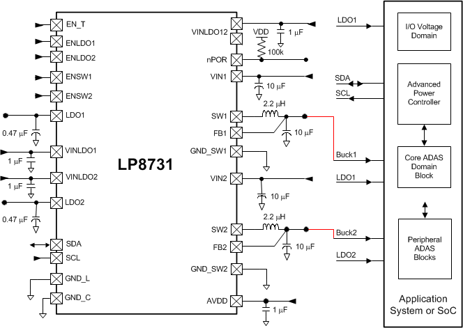 Figure 25. LP8731-Q1 Simplified Schematic
9.2.1 Design Requirements
Table 5. Design Parameters
| DESIGN PARAMETER | EXAMPLE VALUE |
|---|---|
| Input voltage range | 2.8 V to 5.5 V |
| Switching frequency | 2 MHz ±10% |
| Output voltage range: bucks | 0.8875 V to 1.675 V |
| Output current rating: bucks | 1.2 A |
| Output voltage range: LDOs | 0.8 V to 3.3 V |
| Output current rating: LDOs | 300 mA |
| Transient response at max load with Tr = Tf = 10 µs | ΔVOUT approximately equals ±1% |
| Bucks output typical ripple voltage | < 10 mV PWM, < 20 mV PFM |
9.2.2 Detailed Design Procedure
9.2.2.1 Component Selection
9.2.2.1.1 Inductors for SW1 and SW2
There are two main considerations when choosing an inductor: the inductor should not saturate, and the inductor current ripple is small enough to achieve the desired output voltage ripple. Care should be taken when reviewing the different saturation current ratings that are specified by different manufacturers. Saturation current ratings are typically specified at 25°C, so ratings at maximum ambient temperature of the application should be requested from the manufacturer.
There are two methods to choose the inductor saturation current rating:
9.2.2.1.1.1 Method 1:
The saturation current is greater than the sum of the maximum load current and the worst case average to peak inductor current. This can be written as follows:

where
- IRIPPLE: Average to peak inductor current
- IOUTMAX: Maximum load current
- VIN: Maximum input voltage to the buck
- L: Min inductor value including worse case tolerances (30% drop can be considered for method 1)
- ƒ: Minimum switching frequency (1.6 MHz)
- VOUT: Buck Output voltage
9.2.2.1.1.2 Method 2:
A more conservative and recommended approach is to choose an inductor that has saturation current rating greater than the maximum current limit of 1800 mA for Buck1 and Buck2.
Given a peak-to-peak current ripple (IPP) the inductor needs to be at least:

Table 6. Suggested Inductors
| INDUCTOR | VALUE | UNIT | L × W × H (mm) | DCR | IRMS RATING TYP | VENDORS | PART ID |
|---|---|---|---|---|---|---|---|
| LSW1,2 | 2.2 | µH | 3.2 × 2.5 × 1.2 | 70 mΩ | 2.1 A | Toko | DFE322512C |
| LSW1,2 | 2.2 | µH | 3.2 × 2.5 × 1.55 | 64 mΩ | 1.85 A | Murata | LQH32PN2R2NNCL |
| LSW1,2 | 2.2 | µH | 3.2 × 2.5 × 1.2 | 70 mΩ | 2.1 A | Chilisin | MHCD322512-2R2M-A8DY |
| LSW1,2 | 2.2 | µH | 5.0 × 5.0 × 1.5 | 70 mΩ | 2 A | Taiyo Yuden | NP04SZB 2R2N |
9.2.2.1.2 External Capacitors
The regulators on the LP8731-Q1 require external capacitors for regulator stability. These are specifically designed for portable applications requiring minimum board space and smallest components. These capacitors must be correctly selected for good performance.
9.2.2.2 LDO Capacitor Selection
9.2.2.2.1 Input Capacitor
An input capacitor is required for stability. It is recommended that a 1-μF capacitor be connected between the LDO input pin and ground (this capacitance value may be increased without limit).
This capacitor must be located a distance of not more than 1 cm from the input pin and returned to a clean analog ground. Any good quality ceramic, tantalum, or film capacitor may be used at the input.
NOTE
Tantalum capacitors can suffer catastrophic failures due to surge currents when connected to a low impedance source of power (like a battery or a very large capacitor). If a tantalum capacitor is used at the input, it must be ensured by the manufacturer to have a surge current rating sufficient for the application.
There are no requirements for the ESR (Equivalent Series Resistance) on the input capacitor, but tolerance and temperature coefficient must be considered when selecting the capacitor to ensure the capacitance remains approximately 1 μF over the entire operating temperature range.
9.2.2.2.2 Output Capacitor
The LDOs on the LP8731-Q1 are designed specifically to work with very small ceramic output capacitors. A 0.47-µF ceramic capacitor (temperature types Z5U, Y5V or X7R) with ESR between 5 mΩ to 500 mΩ, is suitable in the application circuit.
It is also possible to use tantalum or film capacitors at the device output, COUT (or VOUT), but these are not as attractive for reasons of size and cost.
The output capacitor must meet the requirement for the minimum value of capacitance and also have an ESR value that is within the range 5 mΩ to 500 mΩ for stability.
9.2.2.2.3 Capacitor Characteristics
The LDOs are designed to work with ceramic capacitors on the output to take advantage of the benefits they offer. For capacitance values in the range of 0.47 µF to 4.7 µF, ceramic capacitors are the smallest, least expensive, and have the lowest ESR values, thus making them best for eliminating high-frequency noise. The ESR of a typical 1-µF ceramic capacitor is in the range of 20 mΩ to 40 mΩ, which easily meets the ESR requirement for stability for the LDOs.
For both input and output capacitors, careful interpretation of the capacitor specification is required to ensure correct device operation. The capacitor value can change greatly, depending on the operating conditions and capacitor type.
In particular, the output capacitor selection should take account of all the capacitor parameters, to ensure that the specification is met within the application. The capacitance can vary with DC bias conditions as well as temperature and frequency of operation. Capacitor values also show some decrease over time due to aging. The capacitor parameters are also dependent on the particular case size, with smaller sizes giving poorer performance figures in general. As an example, Figure 26 is typical graph comparing different capacitor case sizes in a capacitance vs DC bias plot.
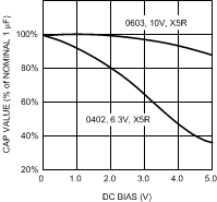 Figure 26. Typical Variation In Capacitance vs DC Bias
As shown in Figure 26, increasing the DC bias condition can result in the capacitance value that falls below the minimum value given in the recommended capacitor specifications table. Note that the graph shows the capacitance out of spec for the 0402 case size capacitor at higher bias voltages. It is therefore recommended that the capacitor manufacturers' specifications for the nominal value capacitor are consulted for all conditions, as some capacitor sizes (e.g. 0402) may not be suitable in the actual application.
The ceramic capacitor’s capacitance can vary with temperature. The capacitor type X7R, which operates over a temperature range of −55°C to 125°C, only varies the capacitance to within ±15%. The capacitor type X5R has a similar tolerance over a reduced temperature range of −55°C to 85°C. Many large value ceramic capacitors, larger than 1 µF are manufactured with Z5U or Y5V temperature characteristics. Their capacitance can drop by more than 50% as the temperature varies from 25°C to 85°C. Therefore X7R is recommended over Z5U and Y5V in applications where the ambient temperature changes significantly above or below 25°C.
Tantalum capacitors are less desirable than ceramic for use as output capacitors because they are more expensive when comparing equivalent capacitance and voltage ratings in the 0.47-µF to 4.7-µF range.
Another important consideration is that tantalum capacitors have higher ESR values than equivalent size ceramics. This means that while it may be possible to find a tantalum capacitor with an ESR value within the stable range, it would have to be larger in capacitance (which means bigger and more costly) than a ceramic capacitor with the same ESR value. It should also be noted that the ESR of a typical tantalum increases about 2:1 as the temperature goes from 25°C down to −40°C, so some guard band must be allowed.
9.2.2.2.4 Input Capacitor Selection for SW1 And SW2
A ceramic input capacitor of 10 µF, 6.3 V is sufficient for the magnetic DC-DC converters. Place the input capacitor as close as possible to the input of the device. A large value may be used for improved input voltage filtering. The recommended capacitor types are X7R or X5R. Y5V type capacitors should not be used. DC bias characteristics of ceramic capacitors must be considered when selecting case sizes like 0805 and 0603. The input filter capacitor supplies current to the PFET switch of the DC-DC converter in the first half of each cycle and reduces voltage ripple imposed on the input power source. A ceramic capacitor’s low Equivalent Series Resistance (ESR) provides the best noise filtering of the input voltage spikes due to fast current transients. A capacitor with sufficient ripple current rating should be selected. The Input current ripple can be calculated as:


The worse case is when VIN = 2 × VOUT.
9.2.2.2.5 Output Capacitor Selection for SW1, SW2
A 10-μF, 6.3-V ceramic capacitor should be used on the output of the SW1 and SW2 magnetic DC-DC converters. The output capacitor needs to be mounted as close as possible to the output of the device. A large value may be used for improved input voltage filtering. The recommended capacitor types are X7R or X5R. Y5V type capacitors should not be used. DC bias characteristics of ceramic capacitors must be considered when selecting case sizes like 0805 and 0603. DC bias characteristics vary from manufacturer to manufacturer and DC bias curves should be requested from them and analyzed as part of the capacitor selection process.
The output filter capacitor of the magnetic DC-DC converter smooths out current flow from the inductor to the load, helps maintain a steady output voltage during transient load changes and reduces output voltage ripple. These capacitors must be selected with sufficient capacitance and sufficiently low ESD to perform these functions.
The output voltage ripple is caused by the charging and discharging of the output capacitor and also due to its ESR and can be calculated as follows:

Voltage peak-to-peak ripple due to ESR can be expressed as follows:
Because the VPP-C and VPP-ESR are out of phase, the rms value can be used to get an approximate value of the peak-to-peak ripple:

NOTE
The output voltage ripple is dependent on the inductor current ripple and the equivalent series resistance of the output capacitor (RESR). The RESR is frequency dependent as well as temperature dependent. The RESR should be calculated with the applicable switching frequency and ambient temperature.
Table 7. Suggested Capacitors
| CAPACITOR | VALUE | L × W × H (mm) | TYPE | TOLERANCE | VENDORS | PART ID |
|---|---|---|---|---|---|---|
| CLDO1, CLDO2 | 0.47 µF | 1.0 × 0.5 × 0.5 (0402) | X7S, 10 V | 10% | Murata | GCM155C71A474KE36 |
| CSW1, CSW2 | 10 µF | 3.2 × 1.6 × 1.6 (1206) | X7R, 16 V | 20% | TDK | C3216XR71C106M |
| CSW1, CSW2 | 10 µF | 2 × 1.25 × 1.45 (0805) | X5R, 16 V | 20% | TDK | CGA4J1X5R1C106M125AC |
| CIN | 1 µF | 0.6 × 0.3 × 0.1 (0603) | X7R, 6.3 V | 20% | TDK | C2012XR71C105K |
| CIN | 1 µF | 1.0 × 0.5× 0.5 (0402) | X7S, 10 V | 10% | Murata | GCM155C71A105KE38 |
9.2.2.2.6 I2C Pull-up Resistor
Both SDA and SCL pins need to have pull-up resistors connected to VINLDO12 or to the power supply of the I2C master. The values of the pull-up resistors (typical approximately1.8 kΩ) are determined by the capacitance of the bus. Too large of a resistor combined with a given bus capacitance results in a rise time that would violate the maximum rise time specification. A too small resistor results in a contention with the pull-down transistor on either slave(s) or master.
9.2.2.2.7 Operation Without I2C Interface
Operation of the LP8731-Q1 without the I2C interface is possible if the system can operate with default values for the LDO and buck regulators. The I2C-less system must rely on the correct default output values of the LDO and Buck converters.
9.2.2.3 Junction Temperature
The maximum junction temperature TJ-MAX-OP is 125°C of the IC package.
The following equations demonstrate junction temperature determination, ambient temperature TA-MAX, and total device power must be controlled to keep TJ below this maximum:
TJ-MAX-OP = TA-MAX + (RθJA) [°C/ Watt] * (PD-MAX) [Watts]
Total IC power dissipation PD-MAX is the sum of the individual power dissipation of the four regulators plus a minor amount for device overhead. Device overhead is Bias, TSD and LDO analog.
PD-MAX = PLDO1 + PLD02 + PBUCK1 + PBUCK2 + (0.0001 A × VIN) [Watts].
Power dissipation of LDO1
PLDO1 = (VINLDO1 – VOUTLDO1) × IOUTLDO1 [V × A]
Power dissipation of LDO2
PLDO2 = (VINLDO2 – VOUTLDO2) × IOUTLDO2 [V × A]
Power dissipation of Buck1
PBuck1 = PIN – POUT =
VOUTBuck1 × IOUTBuck1 × (1 -η1) / η1 [V × A]
η1 = efficiency of buck 1
Power dissipation of Buck2
PBuck2 = PIN – POUT =
VOUTBuck2 × IOUTBuck2 × (1 - η2) / η2 [V × A]
η2 = efficiency of Buck2
Where η is the efficiency for the specific condition taken from efficiency graphs.
9.2.3 Application Curves (LDO)
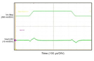
| VIN = 3.6 V to 4.2 V | IOUT = 300 mA | |
| VOUT = 1.8 V | Tr = Tf = 30 µs | |
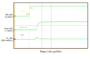
| VIN = 3.6 V | IOUT = 200 mA | |
| VOUT = 1.8 V | EN Tr = 18 ns | |
9.2.4 Application Curves (BUCK)
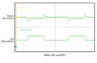
| IOUT = 300 mA to 500 mA PWM | ||
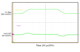
| VIN Step | IOUT = 300 mA | Tr = Tf = 30 µs |