SNVSA28 December 2014 LP8731-Q1
PRODUCTION DATA.
- 1 Features
- 2 Applications
- 3 Description
- 4 Revision History
- 5 Device Comparison Tables
- 6 Pin Configuration and Functions
-
7 Specifications
- 7.1 Absolute Maximum Ratings
- 7.2 ESD Ratings
- 7.3 Recommended Operating Conditions (Bucks)
- 7.4 Thermal Information
- 7.5 General Electrical Characteristics
- 7.6 Low Dropout Regulators, LDO1 And LDO2
- 7.7 Buck Converters SW1, SW2
- 7.8 I/O Electrical Characteristics
- 7.9 Power-On Reset Threshold/Function (POR)
- 7.10 I2C-Compatible Interface Timing
- 7.11 Typical Characteristics
-
8 Detailed Description
- 8.1 Overview
- 8.2 Functional Block Diagram
- 8.3
Features Description
- 8.3.1 Linear Low Dropout Regulators (LDOs)
- 8.3.2 No-Load Stability
- 8.3.3 LDO1 and LDO2 Control Registers
- 8.3.4
SW1, SW2: Synchronous Step-Down Magnetic DC-DC Converters
- 8.3.4.1 Functional Description
- 8.3.4.2 Circuit Operation
- 8.3.4.3 PWM Operation
- 8.3.4.4 Internal Synchronous Rectification
- 8.3.4.5 Current Limiting
- 8.3.4.6 SW1, SW2 Operation
- 8.3.4.7 SW1, SW2 Control Registers
- 8.3.4.8 Shutdown Mode
- 8.3.4.9 Soft Start
- 8.3.4.10 Low Dropout Operation
- 8.3.4.11 Flexible Power Sequencing of Multiple Power Supplies
- 8.3.4.12 Power-Up Sequencing Using the EN_T Function
- 8.3.5 Flexible Power-On Reset (for example, Power Good with Delay)
- 8.3.6 Undervoltage Lockout
- 8.4 Device Functional Modes
- 8.5 Programming
- 8.6
LP8731-Q1 Register Maps
- 8.6.1 Interrupt Status Register (ISRA) 0x02
- 8.6.2 System Control 1 Register (SCR1) 0x07
- 8.6.3 EN_DLY Preset Delay Sequence after EN_T Assertion
- 8.6.4 Buck and LDO Output Voltage Enable Register (BKLDOEN) - 0x10
- 8.6.5 Buck and LDO Status Register (BKLDOSR) - 0x11
- 8.6.6 BUCK Voltage Change Control Register 1 (VCCR) - 0x20
- 8.6.7 BUCK1 Target Voltage 1 Register (B1TV1) - 0x23
- 8.6.8 BUCK1 Target Voltage 2 Register (B1TV2) - 0x24
- 8.6.9 BUCK1 Ramp Control Register (B1RC) - 0x25
- 8.6.10 BUCK2 Target 1 Register (B2TV1) - 0x29
- 8.6.11 BUCK2 Target 2 Register (B2TV2) - 0x2A
- 8.6.12 BUCK2 Ramp Control Register (B2RC) - 0x2B
- 8.6.13 BUCK Function Register (BFCR) - 0x38
- 8.6.14 Spread Spectrum Function
- 8.6.15 LDO1 Control Register (LDO1VCR) - 0x39
- 8.6.16 LDO2 Control Register (LDO2VCR) - 0x3A
- 9 Application and Implementation
- 10Power Supply Recommendations
- 11Layout
- 12Device and Documentation Support
- 13Mechanical, Packaging, and Orderable Information
8 Detailed Description
8.1 Overview
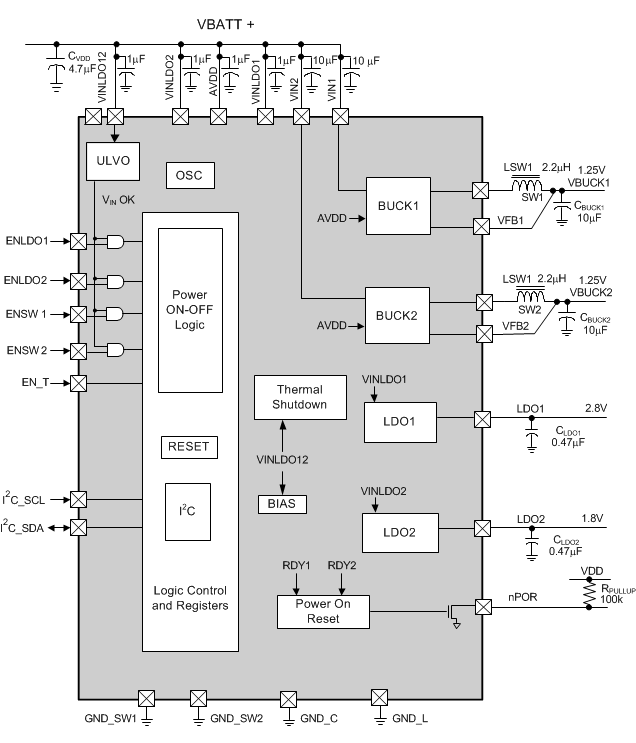
The LP8731-Q1 supplies the various power needs of the application by means of two Linear Low Drop Regulators (LDO1 and LDO2) and two Buck converters (SW1 and SW2). Table 3 lists the output characteristics of the various regulators.
Table 3. Supply Specification
| SUPPLY | LOAD | OUTPUT | ||
|---|---|---|---|---|
| VOUT RANGE (V) | RESOLUTION (mV) | IMAX
MAXIMUM OUTPUT CURRENT (mA) |
||
| LDO1 | analog | 0.8 to 3.3 | 100 | 300 |
| LDO2 | analog | 0.8 to 3.3 | 100 | 300 |
| SW1 | digital | 0.8875 to 1.675 | 12.5 | 1200 |
| SW2 | digital | 0.8875 to 1.675 | 12.5 | 1200 |
8.2 Functional Block Diagram
8.3 Features Description
8.3.1 Linear Low Dropout Regulators (LDOs)
LDO1 and LDO2 are identical linear regulators targeting analog loads characterized by low noise requirements. LDO1 and LDO2 are enabled through the ENLDO pin or through the corresponding LDO1 or LDO2 control register. The output voltages of both LDOs are register programmable. The default output voltages are factory programmed during Final Test, which can be tailored to the specific needs of the system designer.
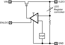 Figure 11. LDO Functional Block Diagram
8.3.2 No-Load Stability
The LDOs remain stable and in regulation with no external load. This is an important consideration in some circuits, for example, CMOS RAM keep-alive applications.
8.3.3 LDO1 and LDO2 Control Registers
LDO1 and LDO2 can be configured by means of the LDO1 and LDO2 control registers. The output voltage is programmable in steps of 100 mV from 1 V to 3.5 V by programming bits D4 to D0 in the LDO Control registers. Both LDO1 and LDO2 are enabled by applying a logic 1 to the ENLDO1 and ENLDO2 pin. Enable/disable control is also provided through enable bit of the LDO1 and LDO2 control registers. The value of the enable LDO bit in the register is logic 1 by default. The output voltage can be altered while the LDO is enabled.
8.3.4 SW1, SW2: Synchronous Step-Down Magnetic DC-DC Converters
8.3.4.1 Functional Description
The LP8731-Q1 incorporates two high-efficiency synchronous switching buck regulators, SW1 and SW2, that deliver a constant voltage from a single Li-Ion battery to the portable system processors. Using a voltage mode architecture with synchronous rectification, both bucks have the ability to deliver up to 1200 mA, depending on the input voltage and output voltage (voltage head room), and the inductor chosen (maximum current capability).
Both SW1 and SW2 can operate up to a 100% duty cycle (PMOS switch always on) for low dropout control of the output voltage. In this way the output voltage is controlled down to the lowest possible input voltage.
Additional features include soft-start, undervoltage lockout, current overload protection, and thermal overload protection.
8.3.4.2 Circuit Operation
A buck converter contains a control block, a switching PFET connected between input and output, a synchronous rectifying NFET connected between the output and ground (BUCKGND pin) and a feedback path. During the first portion of each switching cycle, the control block turns on the internal PFET switch. This allows current to flow from the input through the inductor to the output filter capacitor and load. The inductor limits the current to a ramp with a slope of

by storing energy in a magnetic field. During the second portion of each cycle, the control block turns the PFET switch off, blocking current flow from the input, and then turns the NFET synchronous rectifier on. The inductor draws current from ground through the NFET to the output filter capacitor and load, which ramps the inductor current down with a slope of

The output filter stores charge when the inductor current is high, and releases it when low, smoothing the voltage across the load.
8.3.4.3 PWM Operation
During PWM operation the converter operates as a voltage-mode controller with input voltage feed forward. This allows the converter to achieve excellent load and line regulation. The DC gain of the power stage is proportional to the input voltage. To eliminate this dependence, a feedforward voltage inversely proportional to the input voltage is introduced.
8.3.4.4 Internal Synchronous Rectification
While in PWM mode, the buck uses an internal NFET as a synchronous rectifier to reduce rectifier forward voltage drop and associated power loss. Synchronous rectification provides a significant improvement in efficiency whenever the output voltage is relatively low compared to the voltage drop across an ordinary rectifier diode.
8.3.4.5 Current Limiting
A current limit feature allows the converter to protect itself and external components during overload conditions. PWM mode implements current limiting using an internal comparator that trips at 1.7 A for Buck1 and Buck2 (typical). If the output is shorted to ground the device enters a timed current limit mode where the NFET is turned on for a longer duration until the inductor current falls below a low threshold, ensuring inductor current has more time to decay, thereby preventing runaway.
8.3.4.6 SW1, SW2 Operation
SW1 and SW2 have selectable output voltages ranging from 0.8875 V to 1.675 V (typ.). Both SW1 and SW2 in the LP8731-Q1 are I2C register controlled and are enabled by default through the internal state machine of the LP8731-Q1 following a power-on event that moves the operating mode to the Active state. (See Flexible Power Sequencing of Multiple Power Supplies.) The SW1 and SW2 output voltages revert to default values when the power-on sequence has been completed. The default output voltage for each buck converter is factory programmable. (See Application and Implementation.)
8.3.4.7 SW1, SW2 Control Registers
SW1, SW2 can be enabled/disabled through the corresponding control register.
8.3.4.8 Shutdown Mode
During shutdown the PFET switch, reference, control and bias circuitry of the converters are turned off. The NFET switch is on in shutdown to discharge the output. When the converter is enabled, soft start is activated. It is recommended to disable the converter during the system power up and undervoltage conditions when the supply is less than 2.8 V.
8.3.4.9 Soft Start
The soft-start feature allows the power converter to gradually reach the initial steady state operating point, thus reducing startup stresses and surges. The two LP8731-Q1 buck converters have a soft-start circuit that limits in-rush current during start-up. During start-up the switch current limit is increased in steps. Soft start is activated only if EN goes from logic low to logic high after VIN reaches 2.8 V. Soft start is implemented by increasing switch current limit in steps of 180 mA, 300 mA, and 720 mA for Buck1; 180 mA, 300 mA and 720 mA for Buck2 (typical switch current limit). The start-up time thereby depends on the output capacitor and load current demanded at start-up.
8.3.4.10 Low Dropout Operation
The LP8731-Q1 can operate at 100% duty cycle (no switching; PMOS switch completely on) for low dropout support of the output voltage. In this way the output voltage is controlled down to the lowest possible input voltage. When the device operates near 100% duty cycle, output voltage ripple is approximately 25 mV. The minimum input voltage needed to support the output voltage is
where
- ILOAD: Load current
- RDSON, PFET: Drain to source resistance of PFET switch in the triode region
- RINDUCTOR: Inductor resistance
8.3.4.11 Flexible Power Sequencing of Multiple Power Supplies
The LP8731-Q1 provides several options for power on sequencing. The two bucks can be individually controlled with ENSW1 and ENSW2. The two LDOs can also be individually controlled with ENLDO1 and ENLDO2.
If the user desires a set power-on sequence, the device can be programmed through I2C by raising EN_T from LOW to HIGH.
8.3.4.12 Power-Up Sequencing Using the EN_T Function
EN_T assertion causes the LP8731-Q1 to emerge from Standby mode to Full Operation mode at a preset timing sequence. By default, the enables for the LDOs and Bucks (ENLDO1, ENLDO2, EN_T, ENSW1, ENSW2) are internally pulled down by a 500-kΩ resistor, which causes the part to stay OFF until enabled. If the user wishes to use the preset timing sequence to power on the regulators, transition the EN_T pin from LOW to HIGH. Otherwise, simply tie the enables of each specific regulator HIGH to turn on automatically.
EN_T is edge triggered with rising edge signaling the device to power on. The EN_T input is deglitched, and the default is set at 1 ms. As shown in Figure 12 and Figure 13, a rising EN_T edge starts a power-on sequence, while a falling EN_T edge starts a shutdown sequence. If EN_T is high, toggling the external enables of the regulators has no effect on the device.
The regulators can also be programmed through I2C to turn on and off. By default, I2C enables for the regulators on ON.
The regulators are on following the pattern: Regulators on = (I2C enable) AND (External pin enable OR EN_T high).
NOTE
The EN_T power-up sequencing may also be employed immediately after VIN is applied to the device. However, VIN must be stable for approximately 8 ms minimum before EN_T be asserted high to ensure internal bias, reference, and the Flexible POR timing are stabilized. This initial EN_T delay is necessary only upon first time device power on for power-sequencing function to operate properly.
 Figure 12. Enable Logic Diagram
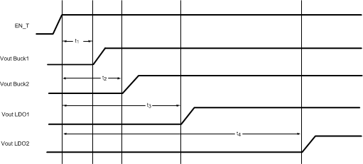 Figure 13. LP8731-Q1 Default Power-Up Sequence
Table 4. Power-On Timing Specification
| MIN | NOM | MAX | UNIT | ||
|---|---|---|---|---|---|
| t1 | Programmable delay from EN_T assertion to VCC_Buck1 on | 1.5 | ms | ||
| t2 | Programmable delay from EN_T assertion to VCC_Buck2 on | 2 | ms | ||
| t3 | Programmable delay from EN_T assertion to VCC_LDO1 on | 3 | ms | ||
| t4 | Programmable delay from EN_T assertion to VCC_LDO2 on | 6 | ms | ||
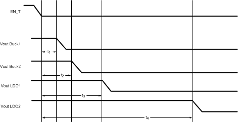 Figure 14. LP8731-Q1 Default Power-Off Sequence
| MIN | NOM | MAX | UNIT | ||
|---|---|---|---|---|---|
| t1 | Programmable delay from EN_T deassertion to VCC_Buck1 off | 1.5 | ms | ||
| t2 | Programmable delay from EN_T deassertion to VCC_Buck2 off | 2 | ms | ||
| t3 | Programmable delay from EN_T deassertion to VCC_LDO1 off | 3 | ms | ||
| t4 | Programmable delay from EN_T deassertion to VCC_LDO2 off | 6 | ms |
NOTE
The LP8731-Q1 default power-off delay setting is the same as the on sequence.
8.3.5 Flexible Power-On Reset (for example, Power Good with Delay)
The LP8731-Q1 is equipped with an internal Power-On-Reset (“POR”) circuit which monitors the output voltage levels on bucks 1 and 2. The nPOR is an open-drain logic output which is logic LOW when either of the buck outputs are below 91% of the rising value, or when one or both outputs fall below 82% of the desired value. The time delay between output voltage level and when nPOR is enabled is (50 µs, 50 ms, 100 ms, 200 ms), 50 µs by default. The system designer can choose the external pull-up resistor (for example, 100 kΩ) for the nPOR pin.
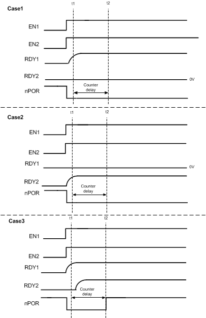 Figure 15. nPOR With Counter Delay
Figure 15 shows the simplest application of the Power-On Reset, where both switcher enables are tied together. In Case 1, EN1 causes nPOR to transition LOW and triggers the nPOR delay counter. If the power supply for Buck2 does not come on within that period, nPOR stays LOW, indicating a power fail mode. Case 2 indicates the vice-versa scenario if Buck1 supply did not come on. In both cases the nPOR remains LOW.
Case 3 shows a typical application of the Power On Reset, where both switcher enables are tied together. Even if RDY1 ramps up slightly faster than RDY2 (or vice versa), then nPOR signal triggers a programmable delay before going HIGH, as explained in Figure 16.
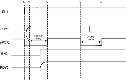 Figure 16. Faults Occurring in Counter Delay after Start-Up
The Figure 16 timing diagram details the power-good with delay with respect to the enable signals EN1, and EN2. The RDY1, RDY2 are internal signals derived from the output of two comparators. Each comparator has been trimmed as follows:
| COMPARATOR LEVEL | BUCK SUPPLY LEVEL |
|---|---|
| HIGH | Greater than 94% |
| LOW | Less than 85% |
The circuits for EN1 and RDY1 are symmetrical to EN2 and RDY2, so each reference to EN1 and RDY1 also works for EN2 and RDY2 and vice versa.
If EN1 and RDY1 signals are HIGH at time t1, then the RDY1 signal rising edge triggers the programmable delay counter (50 μs, 50 ms, 100 ms, 200 ms). This delay forces nPOR LOW between time interval t1 and t2. nPOR is then pulled HIGH after the programmable delay is completed. If EN2 and RDY2 are initiated during this interval, the nPOR signal ignores this event.
If either RDY1or RDY2 were to go LOW at t3 then the programmable delay is triggered again.
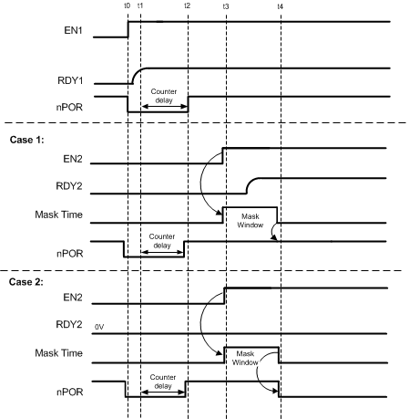 Figure 17. nPOR Mask Window
If the EN1 and RDY1 are initiated in normal operation, then nPOR is asserted and deasserted .
Case 1 in Figure 17 shows a case where EN2 and RDY2 are initiated after triggered programmable delay. To prevent the nPOR being asserted again, a masked window (5 ms) counter delay is triggered off the EN2 rising edge. nPOR is still held HIGH for the duration of the mask, whereupon the nPOR status afterwards depends on the status of both RDY1 and RDY2 lines.
Case 2 shows the case where EN2 is initiated after the RDY1 triggered programmable delay, but RDY2 never goes HIGH (Buck2 never turns on). Normal operation of nPOR occurs with respect to EN1 and RDY1, and the nPOR signal is held HIGH for the duration of the mask window. nPOR goes LOW after the masking window has timed out because it is now dependent on RDY1 and RDY2, where RDY2 is LOW.
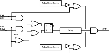 Figure 18. Design Implementation Of The Flexible Power-On Reset
An internal power-on reset of the device is used with EN1 and EN2 to produce a reset signal (LOW) to the delay timer nPOR. EN1 and RDY1 or EN2 and RDY2 are used to generate the set signal (HIGH) to the delay timer. S = R = 1 never occurs. The mask timers are triggered by EN1 and EN2 which are gated with RDY1 and RDY2 to generate outputs to the final AND gate to generate the nPOR.
8.3.6 Undervoltage Lockout
The LP8731-Q1 features an undervoltage lockout circuit. The function of this circuit is to continuously monitor the raw input supply voltage (VINLDO12) and automatically disables the four voltage regulators whenever this supply voltage is less than 2.8 VDC.
The circuit incorporates a bandgap-based circuit that establishes the reference used to determine the 2.8-VDC trip point for a VIN OK – Not OK detector. This VIN OK signal is then used to gate the enable signals to the four regulators of the LP8731-Q1. When VINLDO12 is greater than 2.8 VDC, the four enables control the four regulators, when VINLDO12 is less than 2.8 VDC, the four regulators are disabled by the VIN detector being in the “Not OK” state. The circuit has built-in hysteresis to prevent chattering from occurring.
8.4 Device Functional Modes
8.4.1 Shutdown Mode
During shutdown the PFET switch, reference, control, and bias circuitry of the converters are turned off. The NFET switch is turned on during shutdown to discharge the output. When the converter is enabled, soft start is activated. It is recommended that the converter be disabled during the system power up and undervoltage conditions when the supply is less than 2.8 V.
8.5 Programming
8.5.1 I2C-Compatible Serial Interface
8.5.1.1 I2C Signals
The LP8731-Q1 features an I2C-compatible serial interface, using two dedicated pins: SCL and SDA for I2C clock and data, respectively. Both signals need a pullup resistor according to the I2C specification. The LP8731-Q1 interface is an I2C slave that is clocked by the incoming SCL clock.
Signal timing specifications are according to the I2C bus specification. The maximum bit rate is 400 kbit/s. See I2C specification from NXP Semiconductors for further details.
8.5.1.2 I2C Data Validity
The data on the SDA line must be stable during the HIGH period of the clock signal (SCL), that is, the state of the data line can only be changed when CLK is LOW.
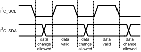 Figure 19. I2C Signals: Data Validity
8.5.1.3 I2C Start and Stop Conditions
START and STOP bits classify the beginning and the end of the I2C session. START condition is defined as the SDA signal transitioning from HIGH to LOW while the SCL line is HIGH. STOP condition is defined as the SDA transitioning from LOW to HIGH while the SCL is HIGH. The I2C master always generates START and STOP bits. The I2C bus is considered to be busy after START condition and free after STOP condition. During data transmission, I2C master can generate repeated START conditions. First START and repeated START conditions are equivalent, function-wise.
 Figure 20. Start And Stop Conditions
8.5.1.4 Transferring Data
Every byte put on the SDA line must be eight bits long, with the most significant bit (MSB) being transferred first. Each byte of data has to be followed by an acknowledge bit. The acknowledged related clock pulse is generated by the master. The transmitter releases the SDA line (HIGH) during the acknowledge clock pulse. The receiver must pull down the SDA line during the 9th clock pulse, signifying acknowledgment. A receiver which has been addressed must generate an acknowledgment (“ACK”) after each byte has been received.
After the START condition, the I2C master sends a chip address. This address is seven bits long followed by an eighth bit which is a data direction bit (R/W).
NOTE
According to industry I2C standards for 7-bit addresses, the MSB of an 8-bit address is removed, and communication actually starts with the 7th most significant bit. For the eighth bit (LSB), a “0” indicates a WRITE and a “1” indicates a READ. The second byte selects the register to which the data is written. The third byte contains data to write to the selected register.
The LP8731-Q1 has factory-programmed I2C addresses. The device has a chip address of 59'h.
 Figure 21. I2C Chip Address (see NOTE above)
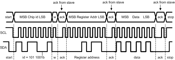
r = read (SDA = “1”)
ack = acknowledge (SDA pulled down by either master or slave)
rs = repeated start
id = LP8731-Q1 chip address: 0x59
When a READ function is to be accomplished, a WRITE function must precede the READ function, as shown in the Read Cycle waveform.
 Figure 23. I2C Read Cycle
8.6 LP8731-Q1 Register Maps
| REGISTER ADDRESS | REGISTER NAME | READ/WRITE | REGISTER DESCRIPTION |
|---|---|---|---|
| 0x02 | ICRA | R | Interrupt Status Register A |
| 0x07 | SCR1 | R/W | System Control 1 Register |
| 0x10 | BKLDOEN | R/W | Buck and LDO Output Voltage Enable Register |
| 0x11 | BKLDOSR | R | Buck and LDO Output Voltage Status Register |
| 0x20 | VCCR | R/W | Voltage Change Control Register 1 |
| 0x23 | B1TV1 | R/W | Buck1 Target Voltage 1 Register |
| 0x24 | B1TV2 | R/W | Buck1 Target Voltage 2 Register |
| 0x25 | B1RC | R/W | Buck1 Ramp Control |
| 0x29 | B2TV1 | R/W | Buck2 Target Voltage 1 Register |
| 0x2A | B2TV2 | R/W | Buck2 Target Voltage 2 Register |
| 0x2B | B2RC | R/W | Buck2 Ramp Control |
| 0x38 | BFCR | R/W | Buck Function Register |
| 0x39 | LDO1VCR | R/W | LDO1 Voltage control Registers |
| 0x3A | LDO2VCR | R/W | LDO2 Voltage control Registers |
8.6.1 Interrupt Status Register (ISRA) 0x02
This register informs the system engineer of the temperature status of the chip.
| D7-D2 | D1 | D0 | |
|---|---|---|---|
| Name | — | Temp 125°C | — |
| Access | — | R | — |
| Data | Reserved | Status bit for thermal warning PMIC T > 125°C 0 – PMIC Temp. < 125°C 1 – PMIC Temp. > 125°C |
Reserved |
| Reset | 0 | 0 | 0 |
8.6.2 System Control 1 Register (SCR1) 0x07
This register allows the user to select the preset delay sequence for power-on timing and to select between an internal and external clock for the bucks.
| D7 | D6-D4 | D3 | D2 | D1 | D0 | |
|---|---|---|---|---|---|---|
| Name | — | EN_DLY | — | FPWM2(1) | FPWM1(1) | ECEN |
| Access | — | R/W | — | R/W | R/W | R/W |
| Data | Reserved | Selects the preset delay sequence from EN_T assertion (shown below) |
Reserved | Buck2 PWM /PFM Mode select 0 – Auto Switch PFM - PWM operation 1 – PWM Mode Only |
Buck 1 PWM /PFM Mode select 0 – Auto Switch PFM - PWM operation 1 – PWM Mode Only |
Reserved |
| Reset | 0 | Factory-Programmed Default | 1 | Factory-Programmed Default | Factory-Programmed Default | 0 |
8.6.3 EN_DLY Preset Delay Sequence after EN_T Assertion
| EN_DLY<2:0> | DELAY (ms) | |||
|---|---|---|---|---|
| Buck1 | Buck2 | LDO1 | LDO2 | |
| 000 | 1 | 1 | 1 | 1 |
| 001 | 1 | 1.5 | 2 | 2 |
| 010 | 1.5 | 2 | 3 | 6 |
| 011 | 1.5 | 2 | 1 | 1 |
| 100 | 1.5 | 2 | 3 | 6 |
| 101 | 1.5 | 1.5 | 2 | 2 |
| 110 | 3 | 2 | 1 | 1.5 |
| 111 | 2 | 3 | 6 | 11 |
8.6.4 Buck and LDO Output Voltage Enable Register (BKLDOEN) – 0x10
This register controls the enables for the Bucks and LDOs.
| D7 | D6 | D5 | D4 | D3 | D2 | D1 | D0 | |
|---|---|---|---|---|---|---|---|---|
| Name | — | LDO2EN | — | LDO1EN | — | BK2EN | — | BK1EN |
| Access | — | R/W | — | R/W | — | R/W | — | R/W |
| Data | Reserved | 0 – Disable 1 – Enable |
Reserved | 0 – Disable 1 – Enable |
Reserved | 0 – Disable 1 – Enable |
Reserved | 0 – Disable 1 – Enable |
| Reset | 0 | 1 | 1 | 1 | 0 | 1 | 0 | 1 |
8.6.5 Buck and LDO Status Register (BKLDOSR) – 0x11
This register monitors whether the Bucks and LDOs meet the voltage output specifications.
| D7 | D6 | D5 | D4 | D3 | D2 | D1 | D0 | |
|---|---|---|---|---|---|---|---|---|
| Name | BKS_OK | LDOS_OK | LDO2_OK | LDO1_OK | — | BK2_OK | — | BK1_OK |
| Access | R | R | R | R | — | R | — | R |
| Data | 0 – Buck 1-2 Not Valid 1 – Bucks Valid |
0 – LDO 1-2 Not Valid 1 – LDOs Valid |
0 – LDO2 Not Valid 1 – LDO2 Valid |
0 – LDO1 Not Valid 1 – LDO1 Valid |
Reserved | 0 – Buck2 Not Valid 1 – Buck2 Valid |
Reserved | 0 – Buck1 Not Valid 1 – Buck1 Valid |
| Reset | 0 | 0 | 0 | 0 | 0 | 0 | 0 | 0 |
8.6.6 BUCK Voltage Change Control Register 1 (VCCR) – 0x20
This register selects and controls the output target voltages for the buck regulators.
| D7-D6 | D5 | D4 | D3-2 | D1 | D0 | |
|---|---|---|---|---|---|---|
| Name | — | B2VS | B2GO | — | B1VS | B1GO |
| Access | — | R/W | R/W | — | R/W | R/W |
| Data | Reserved | Buck2 Target Voltage Select 0 – B2VT1 1 – B2VT2 |
Buck2 Voltage Ramp CTRL 0 – Hold 1 – Ramp to B2VS selection |
Reserved | Buck1 Target Voltage Select 0 – B1VT1 1 – B1VT2 |
Buck1 Voltage Ramp CTRL 0 – Hold 1 – Ramp to B1VS selection |
| Reset | 00 | 0 | 0 | 00 | 0 | 0 |
8.6.7 BUCK1 Target Voltage 1 Register (B1TV1) – 0x23
This register allows the user to program the output target voltage of Buck1 (target voltage 1).
| D7-D6 | D5 | D4-0 | BUCK1 OUTPUT VOLTAGE (V) | |
|---|---|---|---|---|
| Name | — | Buck1 12p5 mV step | B1TV1 | — |
| Access | — | R/W | R/W | — |
| Data | Reserved | 1’h0 | 5’h00 | 0.8875 |
| 1'h1 | 5’h00 | 0.9000 | ||
| 1’h0 | 5’h01 | 0.9125 | ||
| 1'h1 | 5’h01 | 0.9250 | ||
| 1’h0 | 5’h02 | 0.9375 | ||
| 1'h1 | 5’h02 | 0.9500 | ||
| 1’h0 | 5’h03 | 0.9625 | ||
| 1'h1 | 5’h03 | 0.9750 | ||
| 1’h0 | 5’h04 | 0.9875 | ||
| 1'h1 | 5’h04 | 1.0000 | ||
| 1’h0 | 5’h05 | 1.0125 | ||
| 1'h1 | 5’h05 | 1.0250 | ||
| 1’h0 | 5’h06 | 1.0375 | ||
| 1'h1 | 5’h06 | 1.0500 | ||
| 1’h0 | 5’h07 | 1.0625 | ||
| 1'h1 | 5’h07 | 1.0750 | ||
| 1’h0 | 5’h08 | 1.0875 | ||
| 1'h1 | 5’h08 | 1.1000 | ||
| 1’h0 | 5’h09 | 1.1125 | ||
| 1'h1 | 5’h09 | 1.1250 | ||
| 1’h0 | 5’h0A | 1.1375 | ||
| 1'h1 | 5’h0A | 1.1500 | ||
| 1’h0 | 5’h0B | 1.1625 | ||
| 1'h1 | 5’h0B | 1.1750 | ||
| 1’h0 | 5’h0C | 1.1875 | ||
| 1'h1 | 5’h0C | 1.2000 | ||
| 1’h0 | 5’h0D | 1.2125 | ||
| 1'h1 | 5’h0D | 1.2250 | ||
| 1’h0 | 5’h0E | 1.2375 | ||
| 1'h1 | 5’h0E | 1.2500 | ||
| 1’h0 | 5’h0F | 1.2625 | ||
| 1'h1 | 5’h0F | 1.2750 | ||
| Data | Register | 1’h0 | 5'h10 | 1.2875 |
| 1'h1 | 5'h10 | 1.3000 | ||
| 1’h0 | 5'h11 | 1.3125 | ||
| 1’h0 | 5'h11 | 1.3250 | ||
| 1'h1 | 5'h12 | 1.3375 | ||
| 1’h0 | 5'h12 | 1.3500 | ||
| 1'h1 | 5'h13 | 1.3625 | ||
| 1’h0 | 5'h13 | 1.3750 | ||
| 1'h1 | 5'h14 | 1.3875 | ||
| 1’h0 | 5'h14 | 1.4000 | ||
| 1'h1 | 5'h15 | 1.4125 | ||
| 1’h0 | 5'h15 | 1.4250 | ||
| 1'h1 | 5'h16 | 1.4375 | ||
| 1’h0 | 5'h16 | 1.4500 | ||
| 1'h1 | 5'h17 | 1.4625 | ||
| 1’h0 | 5'h17 | 1.4750 | ||
| 1’h0 | 5'h18 | 1.4875 | ||
| 1'h1 | 5'h18 | 1.5000 | ||
| 1’h0 | 5'h19 | 1.5125 | ||
| 1'h1 | 5'h19 | 1.5250 | ||
| 1’h0 | 5'h1A | 1.5375 | ||
| 1'h1 | 5'h1A | 1.5500 | ||
| 1’h0 | 5'h1B | 1.5625 | ||
| 1'h1 | 5'h1B | 1.5750 | ||
| 1’h0 | 5'h1C | 1.5875 | ||
| 1'h1 | 5'h1C | 1.6000 | ||
| 1'h0 | 5'h1D | 1.6125 | ||
| 1'h1 | 5'h1D | 1.6250 | ||
| 1'h0 | 5'h1E | 1.6375 | ||
| 1'h1 | 5'h1E | 1.6500 | ||
| 1'h0 | 5'h1F | 1.6625 | ||
| 1'h1 | 5'h1F | 1.6750 |
8.6.8 BUCK1 Target Voltage 2 Register (B1TV2) - 0x24
This register allows the user to program the output target voltage of Buck1 (target voltage 2).
| D7-D6 | D5 | D4-D0 | BUCK1 OUTPUT VOLTAGE (V) | |
|---|---|---|---|---|
| Name | — | Buck1 12p5 mV step | B1TV2 | — |
| Access | — | R/W | R/W | — |
| Data | Reserved | 1’h0 | 5’h00 | 0.8875 |
| 1'h1 | 5’h00 | 0.9000 | ||
| 1’h0 | 5’h01 | 0.9125 | ||
| 1'h1 | 5’h01 | 0.9250 | ||
| 1’h0 | 5’h02 | 0.9375 | ||
| 1'h1 | 5’h02 | 0.9500 | ||
| 1’h0 | 5’h03 | 0.9625 | ||
| 1'h1 | 5’h03 | 0.9750 | ||
| 1’h0 | 5’h04 | 0.9875 | ||
| 1'h1 | 5’h04 | 1.0000 | ||
| 1’h0 | 5’h05 | 1.0125 | ||
| 1'h1 | 5’h05 | 1.0250 | ||
| 1’h0 | 5’h06 | 1.0375 | ||
| 1'h1 | 5’h06 | 1.0500 | ||
| 1’h0 | 5’h07 | 1.0625 | ||
| 1'h1 | 5’h07 | 1.0750 | ||
| 1’h0 | 5’h08 | 1.0875 | ||
| 1'h1 | 5’h08 | 1.1000 | ||
| 1’h0 | 5’h09 | 1.1125 | ||
| 1'h1 | 5’h09 | 1.1250 | ||
| 1’h0 | 5’h0A | 1.1375 | ||
| 1'h1 | 5’h0A | 1.1500 | ||
| 1’h0 | 5’h0B | 1.1625 | ||
| 1'h1 | 5’h0B | 1.1750 | ||
| 1’h0 | 5’h0C | 1.1875 | ||
| 1'h1 | 5’h0C | 1.2000 | ||
| 1’h0 | 5’h0D | 1.2125 | ||
| 1'h1 | 5’h0D | 1.2250 | ||
| 1’h0 | 5’h0E | 1.2375 | ||
| 1'h1 | 5’h0E | 1.2500 | ||
| 1’h0 | 5’h0F | 1.2625 | ||
| 1'h1 | 5’h0F | 1.2750 | ||
| Data | Reserved | 1’h0 | 5'h10 | 1.2875 |
| 1'h1 | 5'h10 | 1.3000 | ||
| 1’h0 | 5'h11 | 1.3125 | ||
| 1’h0 | 5'h11 | 1.3250 | ||
| 1'h1 | 5'h12 | 1.3375 | ||
| 1’h0 | 5'h12 | 1.3500 | ||
| 1'h1 | 5'h13 | 1.3625 | ||
| 1’h0 | 5'h13 | 1.3750 | ||
| 1'h1 | 5'h14 | 1.3875 | ||
| 1’h0 | 5'h14 | 1.4000 | ||
| 1'h1 | 5'h15 | 1.4125 | ||
| 1’h0 | 5'h15 | 1.4250 | ||
| 1'h1 | 5'h16 | 1.4375 | ||
| 1’h0 | 5'h16 | 1.4500 | ||
| 1'h1 | 5'h17 | 1.4625 | ||
| 1’h0 | 5'h17 | 1.4750 | ||
| 1’h0 | 5'h18 | 1.4875 | ||
| 1'h1 | 5'h18 | 1.5000 | ||
| 1’h0 | 5'h19 | 1.5125 | ||
| 1'h1 | 5'h19 | 1.5250 | ||
| 1’h0 | 5'h1A | 1.5375 | ||
| 1'h1 | 5'h1A | 1.5500 | ||
| 1’h0 | 5'h1B | 1.5625 | ||
| 1'h1 | 5'h1B | 1.5750 | ||
| 1’h0 | 5'h1C | 1.5875 | ||
| 1'h1 | 5'h1C | 1.6000 | ||
| 1'h0 | 5'h1D | 1.6125 | ||
| 1'h1 | 5'h1D | 1.6250 | ||
| 1'h0 | 5'h1E | 1.6375 | ||
| 1'h1 | 5'h1E | 1.6500 | ||
| 1'h0 | 5'h1F | 1.6625 | ||
| 1'h1 | 5'h1F | 1.6750 |
8.6.9 BUCK1 Ramp Control Register (B1RC) - 0x25
This register allows the user to program the rate of change between the target voltages of Buck1.
| D7 | D6-D4 | D3-D0 | ||
|---|---|---|---|---|
| Name | - - - - | - - - - | B1RS | |
| Access | - - - - | - - - - | R/W | |
| Data | Reserved | Reserved | Data Code | Ramp Rate mV/us |
| 4'h0 | Instant | |||
| 4'h1 | 1 | |||
| 4'h2 | 2 | |||
| 4'h3 | 3 | |||
| 4'h4 | 4 | |||
| 4'h'5 | 5 | |||
| 4'h6 | 6 | |||
| 4'h7 | 7 | |||
| 4'h8 | 8 | |||
| 4'h9 | 9 | |||
| 4'hA | 10 | |||
| 4'hB - 4'hF | 10 | |||
8.6.10 BUCK2 Target 1 Register (B2TV1) - 0x29
This register allows the user to program the output target voltage of Buck2 (target voltage 1).
| D7-D6 | D5 | D4-D0 | BUCK2 OUTPUT VOLTAGE (V) | |
|---|---|---|---|---|
| Name | — | Buck1 12.5 mV step | B2TV1 | — |
| Access | — | R/W | R/W | — |
| Data | Reserved | 1’h0 | 5’h00 | 0.8875 |
| 1'h1 | 5’h00 | 0.9000 | ||
| 1’h0 | 5’h01 | 0.9125 | ||
| 1'h1 | 5’h01 | 0.9250 | ||
| 1’h0 | 5’h02 | 0.9375 | ||
| 1'h1 | 5’h02 | 0.9500 | ||
| 1’h0 | 5’h03 | 0.9625 | ||
| 1'h1 | 5’h03 | 0.9750 | ||
| 1’h0 | 5’h04 | 0.9875 | ||
| 1'h1 | 5’h04 | 1.0000 | ||
| 1’h0 | 5’h05 | 1.0125 | ||
| 1'h1 | 5’h05 | 1.0250 | ||
| 1’h0 | 5’h06 | 1.0375 | ||
| 1'h1 | 5’h06 | 1.0500 | ||
| 1’h0 | 5’h07 | 1.0625 | ||
| 1'h1 | 5’h07 | 1.0750 | ||
| 1’h0 | 5’h08 | 1.0875 | ||
| 1'h1 | 5’h08 | 1.1000 | ||
| 1’h0 | 5’h09 | 1.1125 | ||
| 1'h1 | 5’h09 | 1.1250 | ||
| 1’h0 | 5’h0A | 1.1375 | ||
| 1'h1 | 5’h0A | 1.1500 | ||
| 1’h0 | 5’h0B | 1.1625 | ||
| 1'h1 | 5’h0B | 1.1750 | ||
| 1’h0 | 5’h0C | 1.1875 | ||
| 1'h1 | 5’h0C | 1.2000 | ||
| 1’h0 | 5’h0D | 1.2125 | ||
| 1'h1 | 5’h0D | 1.2250 | ||
| 1’h0 | 5’h0E | 1.2375 | ||
| 1'h1 | 5’h0E | 1.2500 | ||
| 1’h0 | 5’h0F | 1.2625 | ||
| 1'h1 | 5’h0F | 1.2750 | ||
| Data | Reserved | 1’h0 | 5'h10 | 1.2875 |
| 1'h1 | 5'h10 | 1.3000 | ||
| 1’h0 | 5'h11 | 1.3125 | ||
| 1’h0 | 5'h11 | 1.3250 | ||
| 1'h1 | 5'h12 | 1.3375 | ||
| 1’h0 | 5'h12 | 1.3500 | ||
| 1'h1 | 5'h13 | 1.3625 | ||
| 1’h0 | 5'h13 | 1.3750 | ||
| 1'h1 | 5'h14 | 1.3875 | ||
| 1’h0 | 5'h14 | 1.4000 | ||
| 1'h1 | 5'h15 | 1.4125 | ||
| 1’h0 | 5'h15 | 1.4250 | ||
| 1'h1 | 5'h16 | 1.4375 | ||
| 1’h0 | 5'h16 | 1.4500 | ||
| 1'h1 | 5'h17 | 1.4625 | ||
| 1’h0 | 5'h17 | 1.4750 | ||
| 1’h0 | 5'h18 | 1.4875 | ||
| 1'h1 | 5'h18 | 1.5000 | ||
| 1’h0 | 5'h19 | 1.5125 | ||
| 1'h1 | 5'h19 | 1.5250 | ||
| 1’h0 | 5'h1A | 1.5375 | ||
| 1'h1 | 5'h1A | 1.5500 | ||
| 1’h0 | 5'h1B | 1.5625 | ||
| 1'h1 | 5'h1B | 1.5750 | ||
| 1’h0 | 5'h1C | 1.5875 | ||
| 1'h1 | 5'h1C | 1.6000 | ||
| 1'h0 | 5'h1D | 1.6125 | ||
| 1'h1 | 5'h1D | 1.6250 | ||
| 1'h0 | 5'h1E | 1.6375 | ||
| 1'h1 | 5'h1E | 1.6500 | ||
| 1'h0 | 5'h1F | 1.6625 | ||
| 1'h1 | 5'h1F | 1.6750 |
8.6.11 BUCK2 Target 2 Register (B2TV2) - 0x2A
This register allows the user to program the output target voltage of Buck2 (target voltage 2).
| D7-D6 | D5 | D4-D0 | BUCK2 OUTPUT VOLTAGE (V) | |
|---|---|---|---|---|
| Name | — | Buck1 12.5 mV step | B2TV2 | — |
| Access | — | R/W | R/W | — |
| Data | Reserved | 1’h0 | 5’h00 | 0.8875 |
| 1'h1 | 5’h00 | 0.9000 | ||
| 1’h0 | 5’h01 | 0.9125 | ||
| 1'h1 | 5’h01 | 0.9250 | ||
| 1’h0 | 5’h02 | 0.9375 | ||
| 1'h1 | 5’h02 | 0.9500 | ||
| 1’h0 | 5’h03 | 0.9625 | ||
| 1'h1 | 5’h03 | 0.9750 | ||
| 1’h0 | 5’h04 | 0.9875 | ||
| 1'h1 | 5’h04 | 1.0000 | ||
| 1’h0 | 5’h05 | 1.0125 | ||
| 1'h1 | 5’h05 | 1.0250 | ||
| 1’h0 | 5’h06 | 1.0375 | ||
| 1'h1 | 5’h06 | 1.0500 | ||
| 1’h0 | 5’h07 | 1.0625 | ||
| 1'h1 | 5’h07 | 1.0750 | ||
| 1’h0 | 5’h08 | 1.0875 | ||
| 1'h1 | 5’h08 | 1.1000 | ||
| 1’h0 | 5’h09 | 1.1125 | ||
| 1'h1 | 5’h09 | 1.1250 | ||
| 1’h0 | 5’h0A | 1.1375 | ||
| 1'h1 | 5’h0A | 1.1500 | ||
| 1’h0 | 5’h0B | 1.1625 | ||
| 1'h1 | 5’h0B | 1.1750 | ||
| 1’h0 | 5’h0C | 1.1875 | ||
| 1'h1 | 5’h0C | 1.2000 | ||
| 1’h0 | 5’h0D | 1.2125 | ||
| 1'h1 | 5’h0D | 1.2250 | ||
| 1’h0 | 5’h0E | 1.2375 | ||
| 1'h1 | 5’h0E | 1.2500 | ||
| 1’h0 | 5’h0F | 1.2625 | ||
| 1'h1 | 5’h0F | 1.2750 | ||
| Data | Reserved | 1’h0 | 5'h10 | 1.2875 |
| 1'h1 | 5'h10 | 1.3000 | ||
| 1’h0 | 5'h11 | 1.3125 | ||
| 1’h0 | 5'h11 | 1.3250 | ||
| 1'h1 | 5'h12 | 1.3375 | ||
| 1’h0 | 5'h12 | 1.3500 | ||
| 1'h1 | 5'h13 | 1.3625 | ||
| 1’h0 | 5'h13 | 1.3750 | ||
| 1'h1 | 5'h14 | 1.3875 | ||
| 1’h0 | 5'h14 | 1.4000 | ||
| 1'h1 | 5'h15 | 1.4125 | ||
| 1’h0 | 5'h15 | 1.4250 | ||
| 1'h1 | 5'h16 | 1.4375 | ||
| 1’h0 | 5'h16 | 1.4500 | ||
| 1'h1 | 5'h17 | 1.4625 | ||
| 1’h0 | 5'h17 | 1.4750 | ||
| 1’h0 | 5'h18 | 1.4875 | ||
| 1'h1 | 5'h18 | 1.5000 | ||
| 1’h0 | 5'h19 | 1.5125 | ||
| 1'h1 | 5'h19 | 1.5250 | ||
| 1’h0 | 5'h1A | 1.5375 | ||
| 1'h1 | 5'h1A | 1.5500 | ||
| 1’h0 | 5'h1B | 1.5625 | ||
| 1'h1 | 5'h1B | 1.5750 | ||
| 1’h0 | 5'h1C | 1.5875 | ||
| 1'h1 | 5'h1C | 1.6000 | ||
| 1'h0 | 5'h1D | 1.6125 | ||
| 1'h1 | 5'h1D | 1.6250 | ||
| 1'h0 | 5'h1E | 1.6375 | ||
| 1'h1 | 5'h1E | 1.6500 | ||
| 1'h0 | 5'h1F | 1.6625 | ||
| 1'h1 | 5'h1F | 1.6750 |
8.6.12 BUCK2 Ramp Control Register (B2RC) - 0x2B
This register allows the user to program the rate of change between the target voltages of Buck2.
| D7 | D6-D4 | D3-D0 | ||
|---|---|---|---|---|
| Name | - - - - | - - - - | B2RS | |
| Access | - - - - | - - - - | R/W | |
| Data | Reserved | Reserved | Data Code | Ramp Rate mV/us |
| 4'h0 | Instant | |||
| 4'h1 | 1 | |||
| 4'h2 | 2 | |||
| 4'h3 | 3 | |||
| 4'h4 | 4 | |||
| 4'h5 | 5 | |||
| 4'h6 | 6 | |||
| 4'h7 | 7 | |||
| 4'h8 | 8 | |||
| 4'h9 | 9 | |||
| 4'hA | 10 | |||
| 4'hB - 4'hF | 10 | |||
| Reset | 0 | 010 | 1000 | |
8.6.13 BUCK Function Register (BFCR) – 0x38
This register allows the Buck switcher clock frequency to be spread across a wider range, allowing for less Electro-magnetic Interference (EMI). The spread spectrum modulation frequency refers to the rate at which the frequency ramps up and down, centered at 2 MHz.
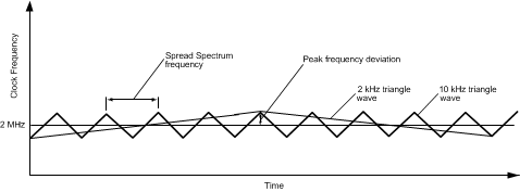 Figure 24. Spread Spectrum Frequency Modulation
8.6.14 Spread Spectrum Function
Periodic switching in the buck regulator is inherently a noisier function block compared to an LDO. It can be challenging in some critical applications to comply with stringent regulatory standards or simply to minimize interference to sensitive circuits in space limited portable systems. The regulator’s switching frequency and harmonics can cause "noise" in the signal spectrum. The magnitude of this noise is measured by its power spectral density. The power spectral density of the switching frequency, FC, is one parameter that system designers want to be as low as practical to reduce interference to the environment and subsystems within their products. The LP8731-Q1 has a user-selectable function on the device, allowing a noise-reduction technique known as spread spectrum to be employed to ease customer’s design and production issues.
The principle behind spread spectrum is to modulate the switching frequency slightly and slowly, and spread the signal frequency over a broader bandwidth. Thus, its power spectral density becomes attenuated, used as a spread spectrum clock via two I2C control register bits bk_ssen, and slomod. With this feature enabled, the intense energy of the clock frequency can be spread across a small band of frequencies in the neighborhood of the center frequency. The results in a reduction of the peak energy!
The LP8731-Q1 spread spectrum clock uses a triangular modulation profile with equal rise and fall slopes. The modulation has the following characteristics:
- The center frequency: FC = 2 MHz, and
- The modulating frequency, ƒM = 6.8 kHz or 12 kHz.
- Peak frequency deviation: Δ_ƒ = ±100 kHz (or ±5%)
- Modulation index β = Δ_ƒ/ƒM = 14.7 or 8.3
This register also allows dynamic scaling of the nPOR Delay Timing. The LP8731-Q1 is equipped with an internal Power-On Reset (POR) circuit which monitors the output voltage levels on the buck regulators, allowing the user to more actively monitor the power status of the device. The undervoltage lockout feature continuously monitor the raw input supply voltage (VINLDO12) and automatically disables the four voltage regulators whenever this supply voltage is less than 2.8 VDC. This prevents the user from damaging the power source (for example, the battery), but can be disabled if the user wishes.
The UVLO feature continuously monitor the raw input supply voltage (VINLDO12) and automatically disables the four voltage regulators whenever this supply voltage is less than 2.8 VDC. This prevents the user from damaging the power source (for example, the battery), but can be disabled if the user wishes.
NOTE
If the supply to VINs is close to 2.8 V with a heavy load current on the regulators, the device could power down due to UVLO. If the user wishes to keep the device active under those conditions, the bypass UVLO feature should be enabled.
| D7-D5 | D4 | D3-D2 | D1 | D0 | |
|---|---|---|---|---|---|
| Name | — | BP_UVLO | TPOR | BK_SLOMOD | BK_SSEN |
| Access | — | R/W | R/W | R/W | R/W |
| Data | Reserved | Bypass UVLO monitoring 0 - Allow UVLO 1 - Disable UVLO |
nPOR Delay Timing 00 - 50 µs 01 - 50 ms 10 - 100 ms 11 - 200 ms |
Buck Spread Spectrum Modulation 0 – 10-kHz triangular wave 1 – 2-kHz triangular wave |
Spread Spectrum Function Output 0 – Disabled 1 – Enabled |
| Reset | 000 | Factory-Programmed Default | 1 | 0 | |
8.6.15 LDO1 Control Register (LDO1VCR) – 0x39
This register allows the user to program the output target voltage of LDO1.
| D7-D5 | D4-D0 | ||
|---|---|---|---|
| Name | — | LDO1_OUT | |
| Access | — | R/W | |
| Data | Reserved | LDO1 Output voltage (V) | |
| 5’h00 | 0.8 | ||
| 5’h01 | 0.9 | ||
| 5’h02 | 1.0 | ||
| 5’h03 | 1.1 | ||
| 5’h04 | 1.2 | ||
| 5’h05 | 1.3 | ||
| 5’h06 | 1.4 | ||
| 5’h07 | 1.5 | ||
| 5’h08 | 1.6 | ||
| 5’h09 | 1.7 | ||
| 5’h0A | 1.8 | ||
| 5’h0B | 1.9 | ||
| 5’h0C | 2.0 | ||
| 5’h0D | 2.1 | ||
| 5’h0E | 2.2 | ||
| 5’h0F | 2.3 | ||
| 5’h10 | 2.4 | ||
| 5’h11 | 2.5 | ||
| 5’h12 | 2.6 | ||
| 5’h13 | 2.7 | ||
| 5’h14 | 2.8 | ||
| 5’h15 | 2.9 | ||
| 5’h16 | 3.0 | ||
| 5’h17 | 3.1 | ||
| 5’h18 | 3.2 | ||
| 5’h19 | 3.3 | ||
8.6.16 LDO2 Control Register (LDO2VCR) – 0x3A
This register allows the user to program the output target voltage of LDO2.
| D7-D5 | D4-D0 | ||
|---|---|---|---|
| Name | — | LDO2_OUT | |
| Access | — | R/W | |
| Data | Reserved | LDO2 Output voltage (V) | |
| 5’h00 | 0.8 | ||
| 5’h01 | 0.9 | ||
| 5’h02 | 1.0 | ||
| 5’h03 | 1.1 | ||
| 5’h04 | 1.2 | ||
| 5’h05 | 1.3 | ||
| 5’h06 | 1.4 | ||
| 5’h07 | 1.5 | ||
| 5’h08 | 1.6 | ||
| 5’h09 | 1.7 | ||
| 5’h0A | 1.8 | ||
| 5’h0B | 1.9 | ||
| 5’h0C | 2.0 | ||
| 5’h0D | 2.1 | ||
| 5’h0E | 2.2 | ||
| 5’h0F | 2.3 | ||
| 5’h10 | 2.4 | ||
| 5’h11 | 2.5 | ||
| 5’h12 | 2.6 | ||
| 5’h13 | 2.7 | ||
| 5’h14 | 2.8 | ||
| 5’h15 | 2.9 | ||
| 5’h16 | 3.0 | ||
| 5’h17 | 3.1 | ||
| 5’h18 | 3.2 | ||
| 5’h19 | 3.3 | ||