SNVSA28 December 2014 LP8731-Q1
PRODUCTION DATA.
- 1 Features
- 2 Applications
- 3 Description
- 4 Revision History
- 5 Device Comparison Tables
- 6 Pin Configuration and Functions
-
7 Specifications
- 7.1 Absolute Maximum Ratings
- 7.2 ESD Ratings
- 7.3 Recommended Operating Conditions (Bucks)
- 7.4 Thermal Information
- 7.5 General Electrical Characteristics
- 7.6 Low Dropout Regulators, LDO1 And LDO2
- 7.7 Buck Converters SW1, SW2
- 7.8 I/O Electrical Characteristics
- 7.9 Power-On Reset Threshold/Function (POR)
- 7.10 I2C-Compatible Interface Timing
- 7.11 Typical Characteristics
-
8 Detailed Description
- 8.1 Overview
- 8.2 Functional Block Diagram
- 8.3
Features Description
- 8.3.1 Linear Low Dropout Regulators (LDOs)
- 8.3.2 No-Load Stability
- 8.3.3 LDO1 and LDO2 Control Registers
- 8.3.4
SW1, SW2: Synchronous Step-Down Magnetic DC-DC Converters
- 8.3.4.1 Functional Description
- 8.3.4.2 Circuit Operation
- 8.3.4.3 PWM Operation
- 8.3.4.4 Internal Synchronous Rectification
- 8.3.4.5 Current Limiting
- 8.3.4.6 SW1, SW2 Operation
- 8.3.4.7 SW1, SW2 Control Registers
- 8.3.4.8 Shutdown Mode
- 8.3.4.9 Soft Start
- 8.3.4.10 Low Dropout Operation
- 8.3.4.11 Flexible Power Sequencing of Multiple Power Supplies
- 8.3.4.12 Power-Up Sequencing Using the EN_T Function
- 8.3.5 Flexible Power-On Reset (for example, Power Good with Delay)
- 8.3.6 Undervoltage Lockout
- 8.4 Device Functional Modes
- 8.5 Programming
- 8.6
LP8731-Q1 Register Maps
- 8.6.1 Interrupt Status Register (ISRA) 0x02
- 8.6.2 System Control 1 Register (SCR1) 0x07
- 8.6.3 EN_DLY Preset Delay Sequence after EN_T Assertion
- 8.6.4 Buck and LDO Output Voltage Enable Register (BKLDOEN) - 0x10
- 8.6.5 Buck and LDO Status Register (BKLDOSR) - 0x11
- 8.6.6 BUCK Voltage Change Control Register 1 (VCCR) - 0x20
- 8.6.7 BUCK1 Target Voltage 1 Register (B1TV1) - 0x23
- 8.6.8 BUCK1 Target Voltage 2 Register (B1TV2) - 0x24
- 8.6.9 BUCK1 Ramp Control Register (B1RC) - 0x25
- 8.6.10 BUCK2 Target 1 Register (B2TV1) - 0x29
- 8.6.11 BUCK2 Target 2 Register (B2TV2) - 0x2A
- 8.6.12 BUCK2 Ramp Control Register (B2RC) - 0x2B
- 8.6.13 BUCK Function Register (BFCR) - 0x38
- 8.6.14 Spread Spectrum Function
- 8.6.15 LDO1 Control Register (LDO1VCR) - 0x39
- 8.6.16 LDO2 Control Register (LDO2VCR) - 0x3A
- 9 Application and Implementation
- 10Power Supply Recommendations
- 11Layout
- 12Device and Documentation Support
- 13Mechanical, Packaging, and Orderable Information
11 Layout
11.1 Layout Guidelines
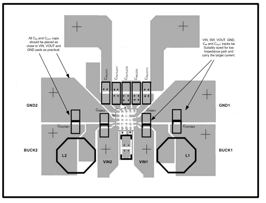
The LP8731-Q1 is a monolithic device with integrated power FETs. For that reason, it is important to pay special attention to the use of appropriate to input, output, power, and ground track dimensions in the PCB layout in order to achieve low impedance small current loop paths and tracks with adequate current density to carry the target currents.
The device pin solder bumps are arranged with power and ground bumps at the edges of the package to facilitate PCB layout considerations. This enables using the top metal layer to route the power and ground tracks. Thus, the current loops for the bucks can be very short and this also makes placing the bypass caps on the device side of the PCB possible. (See Figure 31.) Avoid using vias to tap power and ground planes for the switcher supply pins, because they can be very inductive and could incur large i*dv/dt transient voltage drops. If vias are unavoidable, use them liberally to minimize the impedance they may present.
For more information on board layout techniques, refer to Texas Instruments AN-1112 DSBGA Wafer Level Chip Scale Package (SNVA009). This application note also discusses recommended PCB pad geometry, package handling, solder stencil and the assembly process. See also Texas Instruments AN-1229 SIMPLE SWITCHER® PCB Layout Guidelines (SNVA054) and Texas Instruments AN-2078 PCB Layout for Texas Instrument' SIMPLE SWITCHER® Power Modules (SNVA452).
11.2 Layout Example
 Figure 31. LP8731-Q1 Layout Example