ZHCSDB8A February 2014 – August 2014 LP8754
PRODUCTION DATA.
- 1 特性
- 2 应用
- 3 说明
- 4 修订历史记录
- 5 Pin Configuration and Functions
-
6 Specifications
- 6.1 Absolute Maximum Ratings
- 6.2 ESD Ratings
- 6.3 Recommended Operating Conditions
- 6.4 Thermal Information
- 6.5 General Electrical Characteristics
- 6.6 6-Phase Buck Electrical Characteristics
- 6.7 6-Phase Buck System Characteristics
- 6.8 Protection Features Characteristics
- 6.9 I2C Serial Bus Timing Parameters
- 6.10 Typical Characteristics
-
7 Detailed Description
- 7.1 Overview
- 7.2 Functional Block Diagram
- 7.3 Features Descriptions
- 7.4 Device Functional Modes
- 7.5 Programming
- 7.6
Register Maps
- 7.6.1 Register Descriptions
- 7.6.2 VSET_B0
- 7.6.3 FPWM
- 7.6.4 BUCK0_CTRL
- 7.6.5 BUCK1_CTRL
- 7.6.6 BUCK2_CTRL
- 7.6.7 BUCK3_CTRL
- 7.6.8 BUCK4_CTRL
- 7.6.9 BUCK5_CTRL
- 7.6.10 FLAGS_0
- 7.6.11 FLAGS_1
- 7.6.12 INT_MASK_0
- 7.6.13 GENERAL
- 7.6.14 RESET
- 7.6.15 DELAY_BUCK0
- 7.6.16 CHIP_ID
- 7.6.17 PFM_LEV_B0
- 7.6.18 PHASE_LEV_B0
- 7.6.19 SEL_I_LOAD
- 7.6.20 LOAD_CURR
- 7.6.21 INT_MASK_2
- 8 Application and Implementation
- 9 Power Supply Recommendations
- 10Layout
- 11器件和文档支持
- 12机械封装和可订购信息
8 Application and Implementation
NOTE
Information in the following applications sections is not part of the TI component specification, and TI does not warrant its accuracy or completeness. TI’s customers are responsible for determining suitability of components for their purposes. Customers should validate and test their design implementation to confirm system functionality.
8.1 Application Information
The LP8754 is a multi-phase step-down converter with 6 switcher cores bundled together.
8.2 Typical Application
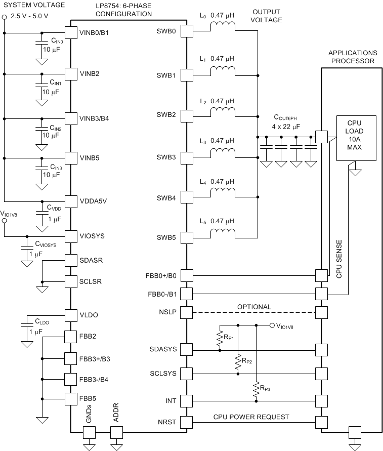 Figure 24. 6-Phase Configuration Schematic
8.2.1 Design Requirements
Table 6 shows requirements for 6-phase configuration.
Table 6. Design Parameters
| DESIGN PARAMETER | EXAMPLE VALUE |
|---|---|
| Input voltage range | 2.5 V to 5 V |
| Output voltage | 1.1 V |
| Converter operation mode | Forced PWM |
| Maximum load current | 10 A |
| Inductor current limit | 2.5 A |
8.2.2 Detailed Design Procedure
The performance of the LP8754 device depends greatly on the care taken in designing the Printed Circuit Board (PCB). The use of low inductance and low serial resistance ceramic capacitors is strongly recommended, while proper grounding is crucial. Attention should be given to decoupling the power supplies. Decoupling capacitors must be connected close to the IC and between the power and ground pins to support high peak currents being drawn from System Power Rail during turn-on of the switching MOSFETs. Keep input and output traces as short as possible, because trace inductance, resistance and capacitance can easily become the performance limiting items. The separate power pins VINBXX are not connected together internally. The VINBXX power connections shall be connected together outside the package using power plane construction.
8.2.2.1 Inductor Selection
The DC bias current characteristics of inductors must be considered. Different manufacturers follow different saturation current rating specifications, so attention must be given to details. (Please request DC bias curves from the manufacturer as part of the inductor selection process.) Minimum effective value of inductance to ensure good performance is 0.25 µH at 2.5 A (Default ILIMITP typical) bias current over the inductor's operating temperature range. The inductor’s DC resistance should be less than 0.05 Ω for good efficiency at high-current condition. The inductor AC loss (resistance) also affects conversion efficiency. Higher Q factor at switching frequency usually gives better efficiency at light load to middle load. Table 7 lists suggested inductors and suppliers. Shielded inductors radiate less noise and are preferable.
Table 7. Suggested Inductors
| ITEM | MODEL | VENDOR | DIMENSIONS LxWxH (mm) | D.C.R (mΩ) MAX |
|---|---|---|---|---|
| L0 to L5; Step-down converter inductor 0.47 µH | LQM21PNR47MGH DFE252012 R47 DFE201612C R47N |
Murata TOKO TOKO |
2.0 x 1.2 x 1.0 2.5 x 2 x 1.2 2.0 x 1.6 x 1.2 |
40 (typ) 39 50 |
8.2.2.2 Input Capacitor Selection
A ceramic input capacitor of 10 µF, 10 V is sufficient for most applications. Place the input capacitor as close as possible to the VINBXX pin and GND pin of the device. A larger value or higher voltage rating may be used to improve input voltage filtering. Use X7R or X5R types, do not use Y5V. DC bias characteristics of ceramic capacitors must be considered when selecting case sizes like 0402. Minimum effective input capacitance to ensure good performance is 2.5 µF at maximum input voltage DC bias including tolerances and over ambient temp range, assuming that there is at least 22 µF of additional capacitance common for all the power input pins on the system power rail.
The input filter capacitor supplies current to the PFET (high-side) switch in the first half of each cycle and reduces voltage ripple imposed on the input power source. A ceramic capacitor's low equivalent series resistance (ESR) provides the best noise filtering of the input voltage spikes due to this rapidly changing current. Select an input filter capacitor with sufficient ripple current rating.
For additional noise immunity, adding a high-frequency decoupling capacitor of 100 nF to 1 µF between VDDA5V pin and GND is recommended.
Table 8. Suggested Input Capacitors (X5R Dielectric)
| MANUFACTURER | PART NUMBER | VALUE | CASE SIZE | VOLTAGE RATING |
|---|---|---|---|---|
| Murata | GRM188R60J106ME84 | 10 µF (20%) | 0603 | 6.3 V |
| TDK | C1608X5R1A106KT | 10 µF (10%) | 0603 | 10 V |
| Taiyo Yuden | LMK107BJ106MALTD | 10 µF (20%) | 0603 | 10 V |
| Samsung | CL10A226MP8NUNE | 22 µF (20%) | 0603 | 10 V |
8.2.2.3 Output Capacitor Selection
Use ceramic capacitor, X7R or X5R types; do not use Y5V. DC bias voltage characteristics of ceramic capacitors must be considered. DC bias characteristics vary from manufacturer to manufacturer, and DC bias curves should be requested from them as part of the capacitor selection process. The output filter capacitor smooths out current flow from the inductor to the load, helps maintain a steady output voltage during transient load changes and reduces output voltage ripple. These capacitors must be selected with sufficient capacitance and sufficiently low ESR to perform these functions. Minimum effective output capacitance to ensure good performance in 6-phase configuration is 30 µF at the output voltage DC bias including tolerances and over ambient temp range.
The output voltage ripple is caused by the charging and discharging of the output capacitor and also due to its RESR. The RESR is frequency dependent (as well as temperature dependent); make sure the value used for selection process is at the switching frequency of the part.
A higher output capacitance improves the load step behavior and reduces the output voltage ripple as well as decreasing the PFM switching frequency. For most 6-phase applications 4 x 22-µF 0603 capacitors for COUT is suitable. Although the converter's loop compensation can be programmed to adapt to virtually several hundreds of microfarads COUT, an effective COUT less than 120 µF is preferred -- there is not necessarily any benefit to having a COUT higher than 120 µF. Note that the output capacitor may be the limiting factor in the output voltage ramp, especially for very large (> 100 µF) output capacitors. For large output capacitors, the output voltage might be slower than the programmed ramp rate at voltage transitions, because of the higher energy stored on the output capacitance. Also at start-up, the time required to charge the output capacitor to target value might be longer. At shutdown, if the output capacitor is discharged by the internal discharge resistor, more time is required to settle VOUT down as a consequence of the increased time constant.
Table 9. Suggested Output Capacitor
| MANUFACTURER | PART NUMBER | VALUE | CASE SIZE | VOLTAGE RATING |
|---|---|---|---|---|
| Samsung | CL10A226MP8NUNE | 22 µF (20%) | 0603 | 10 V |
8.2.2.4 LDO Capacitor Selection
A ceramic low ESR 1-μF capacitor should be connected between the VLDO and GNDA pins.
Table 10. Suggested LDO Capacitor
| MANUFACTURER | PART NUMBER | VALUE | CASE SIZE | VOLTAGE RATING |
|---|---|---|---|---|
| Samsung | CL03A105MQ3CSNH | 1 µF (20%) | 0201 | 6.3 V |
8.2.2.5 VIOSYS Capacitor Selection
Adding a ceramic low ESR 1-μF capacitor between the VIOSYS pin and GND is recommended. If VVIOSYS signal is low noisy the capacitor is not required.
8.2.3 Application Curves
Unless otherwise specified: VVDDA5V = VVINBXX = 3.7 V, VOUT = 1.1 V, TA = 25°C
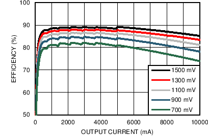
| VIN = 3.7 V | Inductor: Murata LQM21PNR47MGH | |
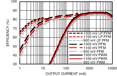
| VOUTSET = 900, 1100 and 1300 mV | ||
| Inductor: Murata LQM21PNR47MGH | ||

| IOUT = 3 A | Inductor: Murata LQM21PNR47MGH | |

| VOUTSET = 1.1 V |
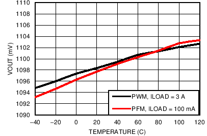
| VOUTSET = 1.1 V |
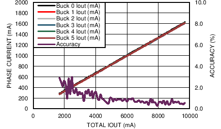
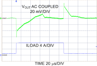
| IOUT 1 A → 8 A → 1 A | tr = tf = 400 ns | |
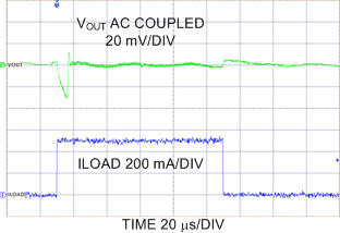
| IOUT 0.5 mA → 0.5 A → 0.5 mA | ||
| tr = tf = 100 ns |
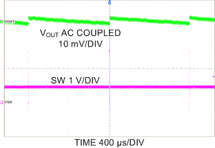
| IOUT = 100 µA |
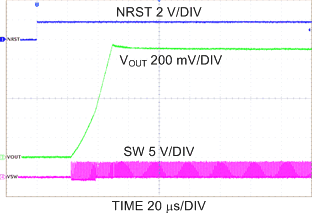
| No Load |
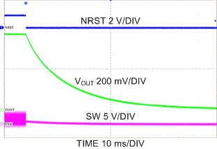
| No Load | ||
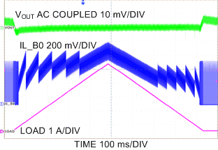
| IOUT 0 A → 5 A → 0 A | ||
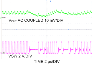
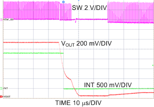
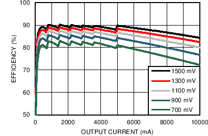
| VIN = 2.7 V | Inductor: Murata LQM21PNR47MGH | |
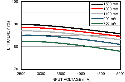
| IOUT = 1 A | ||
| Inductor: Murata LQM21PNR47MGH | ||

| IOUT = 6 A | Inductor: Murata LQM21PNR47MGH | |
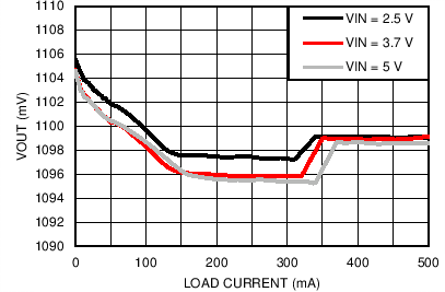
| VOUTSET = 1.1 V |
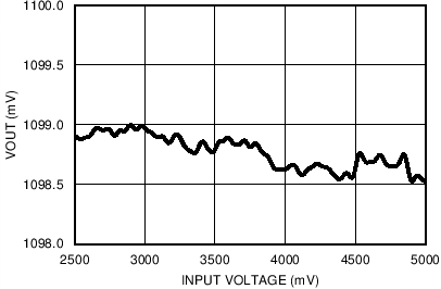
| ILOAD = 1.0 A | VOUTSET = 1.1 V |
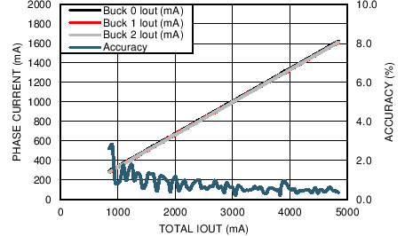
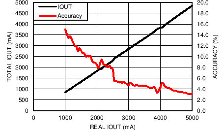
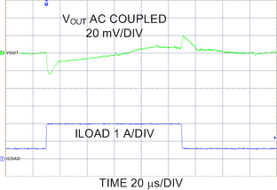
| IOUT 0.6 A → 2 A → 0.6 A | tr = tf = 400 ns | |
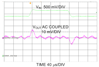
| VIN 3.3 V → 3.8 V → 3.3 V | tr = tf = 10 µs | |
| IOUT = 2000 mA DC | ||
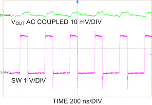
| IOUT = 200 mA |
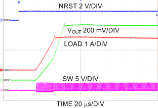
| 3-A Load |
