ZHCSHY8 March   2018 LP87561-Q1 , LP87562-Q1 , LP87563-Q1 , LP87564-Q1 , LP87565-Q1

PRODUCTION DATA.  

  1. 特性
  2. 应用
  3. 说明
    1.     效率与输出电流间的关系
  4. 修订历史记录
  5. Device Comparison Table
  6. Pin Configuration and Functions
    1.     Pin Functions
  7. Specifications
    1. 7.1 Absolute Maximum Ratings
    2. 7.2 ESD Ratings
    3. 7.3 Recommended Operating Conditions
    4. 7.4 Thermal Information
    5. 7.5 Electrical Characteristics
    6. 7.6 I2C Serial Bus Timing Requirements
    7. 7.7 Typical Characteristics
  8. Detailed Description
    1. 8.1 Overview
    2. 8.2 Functional Block Diagram
    3. 8.3 Feature Descriptions
      1. 8.3.1 Multi-Phase DC/DC Converters
        1. 8.3.1.1 Overview
        2. 8.3.1.2 Multiphase Operation, Phase Adding, and Phase-Shedding
        3. 8.3.1.3 Transition Between PWM and PFM Modes
        4. 8.3.1.4 Multiphase Switcher Configurations
        5. 8.3.1.5 Buck Converter Load-Current Measurement
        6. 8.3.1.6 Spread-Spectrum Mode
      2. 8.3.2 Sync Clock Functionality
      3. 8.3.3 Power-Up
      4. 8.3.4 Regulator Control
        1. 8.3.4.1 Enabling and Disabling Regulators
        2. 8.3.4.2 Changing Output Voltage
      5. 8.3.5 Enable and Disable Sequences
      6. 8.3.6 Device Reset Scenarios
      7. 8.3.7 Diagnosis and Protection Features
        1. 8.3.7.1 Power-Good Information (PGOOD Pin)
        2. 8.3.7.2 Warnings for Diagnosis (Interrupt)
          1. 8.3.7.2.1 Output Power Limit
          2. 8.3.7.2.2 Thermal Warning
        3. 8.3.7.3 Protection (Regulator Disable)
          1. 8.3.7.3.1 Short-Circuit and Overload Protection
          2. 8.3.7.3.2 Overvoltage Protection
          3. 8.3.7.3.3 Thermal Shutdown
        4. 8.3.7.4 Fault (Power Down)
          1. 8.3.7.4.1 Undervoltage Lockout
      8. 8.3.8 GPIO Signal Operation
      9. 8.3.9 Digital Signal Filtering
    4. 8.4 Device Functional Modes
      1. 8.4.1 Modes of Operation
    5. 8.5 Programming
      1. 8.5.1 I2C-Compatible Interface
        1. 8.5.1.1 Data Validity
        2. 8.5.1.2 Start and Stop Conditions
        3. 8.5.1.3 Transferring Data
        4. 8.5.1.4 I2C-Compatible Chip Address
        5. 8.5.1.5 Auto-Increment Feature
    6. 8.6 Register Maps
      1. 8.6.1 Register Descriptions
        1. 8.6.1.1  OTP_REV
        2. 8.6.1.2  BUCK0_CTRL1
        3. 8.6.1.3  BUCK0_CTRL2
        4. 8.6.1.4  BUCK1_CTRL1
        5. 8.6.1.5  BUCK1_CTRL2
        6. 8.6.1.6  BUCK2_CTRL1
        7. 8.6.1.7  BUCK2_CTRL2
        8. 8.6.1.8  BUCK3_CTRL1
        9. 8.6.1.9  BUCK3_CTRL2
        10. 8.6.1.10 BUCK0_VOUT
        11. 8.6.1.11 BUCK0_FLOOR_VOUT
        12. 8.6.1.12 BUCK1_VOUT
        13. 8.6.1.13 BUCK1_FLOOR_VOUT
        14. 8.6.1.14 BUCK2_VOUT
        15. 8.6.1.15 BUCK2_FLOOR_VOUT
        16. 8.6.1.16 BUCK3_VOUT
        17. 8.6.1.17 BUCK3_FLOOR_VOUT
        18. 8.6.1.18 BUCK0_DELAY
        19. 8.6.1.19 BUCK1_DELAY
        20. 8.6.1.20 BUCK2_DELAY
        21. 8.6.1.21 BUCK3_DELAY
        22. 8.6.1.22 GPIO2_DELAY
        23. 8.6.1.23 GPIO3_DELAY
        24. 8.6.1.24 RESET
        25. 8.6.1.25 CONFIG
        26. 8.6.1.26 INT_TOP1
        27. 8.6.1.27 INT_TOP2
        28. 8.6.1.28 INT_BUCK_0_1
        29. 8.6.1.29 INT_BUCK_2_3
        30. 8.6.1.30 TOP_STAT
        31. 8.6.1.31 BUCK_0_1_STAT
        32. 8.6.1.32 BUCK_2_3_STAT
        33. 8.6.1.33 TOP_MASK1
        34. 8.6.1.34 TOP_MASK2
        35. 8.6.1.35 BUCK_0_1_MASK
        36. 8.6.1.36 BUCK_2_3_MASK
        37. 8.6.1.37 SEL_I_LOAD
        38. 8.6.1.38 I_LOAD_2
        39. 8.6.1.39 I_LOAD_1
        40. 8.6.1.40 PGOOD_CTRL1
        41. 8.6.1.41 PGOOD_CTRL2
        42. 8.6.1.42 PGOOD_FLT
        43. 8.6.1.43 PLL_CTRL
        44. 8.6.1.44 PIN_FUNCTION
        45. 8.6.1.45 GPIO_CONFIG
        46. 8.6.1.46 GPIO_IN
        47. 8.6.1.47 GPIO_OUT
  9. Application and Implementation
    1. 9.1 Application Information
    2. 9.2 Typical Applications
      1. 9.2.1 Design Requirements
        1. 9.2.1.1 Inductor Selection
        2. 9.2.1.2 Input Capacitor Selection
        3. 9.2.1.3 Output Capacitor Selection
        4. 9.2.1.4 Snubber Components
        5. 9.2.1.5 Supply Filtering Components
        6. 9.2.1.6 Current Limit vs. Maximum Output Current
      2. 9.2.2 Detailed Design Procedure
      3. 9.2.3 Application Curves
  10. 10Power Supply Recommendations
  11. 11Layout
    1. 11.1 Layout Guidelines
    2. 11.2 Layout Example
  12. 12器件和文档支持
    1. 12.1 器件支持
      1. 12.1.1 Third-Party Products Disclaimer
    2. 12.2 文档支持
    3. 12.3 相关链接
    4. 12.4 接收文档更新通知
    5. 12.5 社区资源
    6. 12.6 商标
    7. 12.7 静电放电警告
    8. 12.8 Glossary
  13. 13"机械、封装和可订购信息

封装选项

请参考 PDF 数据表获取器件具体的封装图。

机械数据 (封装 | 引脚)
  • RNF|26
散热焊盘机械数据 (封装 | 引脚)
订购信息

Spread-Spectrum Mode

Systems with periodic switching signals may generate a large amount of switching noise in a set of narrowband frequencies (the switching frequency and its harmonics). The usual solution to decrease noise coupling is to add EMI filters and shields to the boards. The LP8756x-Q1 device has register-selectable spread-spectrum mode which minimizes the need for output filters, ferrite beads, or chokes. In spread-spectrum mode, the switching frequency varies around the center frequency, reducing the EMI emissions radiated by the converter and associated passive components and PCB traces (see Figure 12). This feature is available only when internal RC oscillator is used (PLL_MODE[1:0] = 00 in PLL_CTRL register), and it is enabled with the EN_SPREAD_SPEC bit (PIN_FUNCTION register), and it affects all the buck cores.
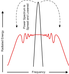
LP87561-Q1 LP87562-Q1 LP87563-Q1 LP87564-Q1 LP87565-Q1 30190611.gif
Where a fixed-frequency converter exhibits large amounts of spectral energy at the switching frequency, the spread-spectrum architecture of the LP8756x-Q1 spreads that energy over a large bandwidth.
Figure 12. Spread-Spectrum Modulation