ZHCSHY8 March 2018 LP87561-Q1 , LP87562-Q1 , LP87563-Q1 , LP87564-Q1 , LP87565-Q1
PRODUCTION DATA.
- 1 特性
- 2 应用
- 3 说明
- 4 修订历史记录
- 5 Device Comparison Table
- 6 Pin Configuration and Functions
- 7 Specifications
-
8 Detailed Description
- 8.1 Overview
- 8.2 Functional Block Diagram
- 8.3
Feature Descriptions
- 8.3.1 Multi-Phase DC/DC Converters
- 8.3.2 Sync Clock Functionality
- 8.3.3 Power-Up
- 8.3.4 Regulator Control
- 8.3.5 Enable and Disable Sequences
- 8.3.6 Device Reset Scenarios
- 8.3.7 Diagnosis and Protection Features
- 8.3.8 GPIO Signal Operation
- 8.3.9 Digital Signal Filtering
- 8.4 Device Functional Modes
- 8.5 Programming
- 8.6
Register Maps
- 8.6.1
Register Descriptions
- 8.6.1.1 OTP_REV
- 8.6.1.2 BUCK0_CTRL1
- 8.6.1.3 BUCK0_CTRL2
- 8.6.1.4 BUCK1_CTRL1
- 8.6.1.5 BUCK1_CTRL2
- 8.6.1.6 BUCK2_CTRL1
- 8.6.1.7 BUCK2_CTRL2
- 8.6.1.8 BUCK3_CTRL1
- 8.6.1.9 BUCK3_CTRL2
- 8.6.1.10 BUCK0_VOUT
- 8.6.1.11 BUCK0_FLOOR_VOUT
- 8.6.1.12 BUCK1_VOUT
- 8.6.1.13 BUCK1_FLOOR_VOUT
- 8.6.1.14 BUCK2_VOUT
- 8.6.1.15 BUCK2_FLOOR_VOUT
- 8.6.1.16 BUCK3_VOUT
- 8.6.1.17 BUCK3_FLOOR_VOUT
- 8.6.1.18 BUCK0_DELAY
- 8.6.1.19 BUCK1_DELAY
- 8.6.1.20 BUCK2_DELAY
- 8.6.1.21 BUCK3_DELAY
- 8.6.1.22 GPIO2_DELAY
- 8.6.1.23 GPIO3_DELAY
- 8.6.1.24 RESET
- 8.6.1.25 CONFIG
- 8.6.1.26 INT_TOP1
- 8.6.1.27 INT_TOP2
- 8.6.1.28 INT_BUCK_0_1
- 8.6.1.29 INT_BUCK_2_3
- 8.6.1.30 TOP_STAT
- 8.6.1.31 BUCK_0_1_STAT
- 8.6.1.32 BUCK_2_3_STAT
- 8.6.1.33 TOP_MASK1
- 8.6.1.34 TOP_MASK2
- 8.6.1.35 BUCK_0_1_MASK
- 8.6.1.36 BUCK_2_3_MASK
- 8.6.1.37 SEL_I_LOAD
- 8.6.1.38 I_LOAD_2
- 8.6.1.39 I_LOAD_1
- 8.6.1.40 PGOOD_CTRL1
- 8.6.1.41 PGOOD_CTRL2
- 8.6.1.42 PGOOD_FLT
- 8.6.1.43 PLL_CTRL
- 8.6.1.44 PIN_FUNCTION
- 8.6.1.45 GPIO_CONFIG
- 8.6.1.46 GPIO_IN
- 8.6.1.47 GPIO_OUT
- 8.6.1
Register Descriptions
- 9 Application and Implementation
- 10Power Supply Recommendations
- 11Layout
- 12器件和文档支持
- 13"机械、封装和可订购信息
8.5.1.3 Transferring Data
Each byte put on the SDA line must be eight bits long, with the most significant bit (MSB) being transferred first. Each byte of data has to be followed by an acknowledge bit. The acknowledge related clock pulse is generated by the master. The master releases the SDA line (HIGH) during the acknowledge clock pulse. The LP8756x-Q1 pulls down the SDA line during the 9th clock pulse, signifying an acknowledge. The LP8756x-Q1 generates an acknowledge after each byte has been received.
There is one exception to the acknowledge after each byte rule. When the master is the receiver, it must indicate to the transmitter an end of data by not-acknowledging (negative acknowledge) the last byte clocked out of the slave. This negative acknowledge still includes the acknowledge clock pulse (generated by the master), but the SDA line is not pulled down.
NOTE
If the NRST signal is low during I2C communication the LP8756x-Q1 device does not drive SDA line. The ACK signal and data transfer to the master is disabled at that time.
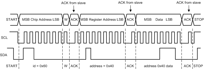
After the START condition, the bus master sends a chip address. This address is seven bits long followed by an eighth bit which is a data direction bit (READ or WRITE). For the eighth bit, a 0 indicates a WRITE, and a 1 indicates a READ. The second byte selects the register to which the data will be written. The third byte contains data to write to the selected register.
 Figure 25. Write Cycle (w = write; SDA = 0), Using Example id = Device Address = 0x60 for LP8756x-Q1
