ZHCSHY8 March 2018 LP87561-Q1 , LP87562-Q1 , LP87563-Q1 , LP87564-Q1 , LP87565-Q1
PRODUCTION DATA.
- 1 特性
- 2 应用
- 3 说明
- 4 修订历史记录
- 5 Device Comparison Table
- 6 Pin Configuration and Functions
- 7 Specifications
-
8 Detailed Description
- 8.1 Overview
- 8.2 Functional Block Diagram
- 8.3
Feature Descriptions
- 8.3.1 Multi-Phase DC/DC Converters
- 8.3.2 Sync Clock Functionality
- 8.3.3 Power-Up
- 8.3.4 Regulator Control
- 8.3.5 Enable and Disable Sequences
- 8.3.6 Device Reset Scenarios
- 8.3.7 Diagnosis and Protection Features
- 8.3.8 GPIO Signal Operation
- 8.3.9 Digital Signal Filtering
- 8.4 Device Functional Modes
- 8.5 Programming
- 8.6
Register Maps
- 8.6.1
Register Descriptions
- 8.6.1.1 OTP_REV
- 8.6.1.2 BUCK0_CTRL1
- 8.6.1.3 BUCK0_CTRL2
- 8.6.1.4 BUCK1_CTRL1
- 8.6.1.5 BUCK1_CTRL2
- 8.6.1.6 BUCK2_CTRL1
- 8.6.1.7 BUCK2_CTRL2
- 8.6.1.8 BUCK3_CTRL1
- 8.6.1.9 BUCK3_CTRL2
- 8.6.1.10 BUCK0_VOUT
- 8.6.1.11 BUCK0_FLOOR_VOUT
- 8.6.1.12 BUCK1_VOUT
- 8.6.1.13 BUCK1_FLOOR_VOUT
- 8.6.1.14 BUCK2_VOUT
- 8.6.1.15 BUCK2_FLOOR_VOUT
- 8.6.1.16 BUCK3_VOUT
- 8.6.1.17 BUCK3_FLOOR_VOUT
- 8.6.1.18 BUCK0_DELAY
- 8.6.1.19 BUCK1_DELAY
- 8.6.1.20 BUCK2_DELAY
- 8.6.1.21 BUCK3_DELAY
- 8.6.1.22 GPIO2_DELAY
- 8.6.1.23 GPIO3_DELAY
- 8.6.1.24 RESET
- 8.6.1.25 CONFIG
- 8.6.1.26 INT_TOP1
- 8.6.1.27 INT_TOP2
- 8.6.1.28 INT_BUCK_0_1
- 8.6.1.29 INT_BUCK_2_3
- 8.6.1.30 TOP_STAT
- 8.6.1.31 BUCK_0_1_STAT
- 8.6.1.32 BUCK_2_3_STAT
- 8.6.1.33 TOP_MASK1
- 8.6.1.34 TOP_MASK2
- 8.6.1.35 BUCK_0_1_MASK
- 8.6.1.36 BUCK_2_3_MASK
- 8.6.1.37 SEL_I_LOAD
- 8.6.1.38 I_LOAD_2
- 8.6.1.39 I_LOAD_1
- 8.6.1.40 PGOOD_CTRL1
- 8.6.1.41 PGOOD_CTRL2
- 8.6.1.42 PGOOD_FLT
- 8.6.1.43 PLL_CTRL
- 8.6.1.44 PIN_FUNCTION
- 8.6.1.45 GPIO_CONFIG
- 8.6.1.46 GPIO_IN
- 8.6.1.47 GPIO_OUT
- 8.6.1
Register Descriptions
- 9 Application and Implementation
- 10Power Supply Recommendations
- 11Layout
- 12器件和文档支持
- 13"机械、封装和可订购信息
8.3.1.2 Multiphase Operation, Phase Adding, and Phase-Shedding
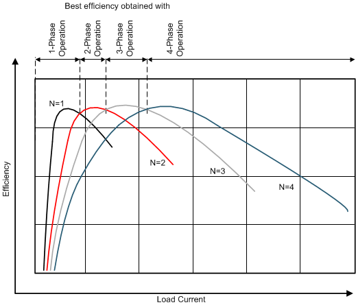
Under heavy load conditions, the 4-phase converter switches each channel 90° apart. As a result, the 4-phase converter has an effective ripple frequency four times greater than the switching frequency of any one phase. In the same way 3-phase converter has an effective ripple frequency three times greater and 2-phase converter has an effective ripple frequency two times greater than the switching frequency of any one phase. However, the parallel operation decreases the efficiency at light load conditions. In order to overcome this operational inefficiency, the LP8756x-Q1 can change the number of active phases to optimize efficiency for the variations of the load. This is called phase adding/shedding. The concept is shown in Figure 11.
The converter can be forced to multiphase operation by the BUCKx_FPWM_MP bit in BUCKx_CTRL1 register. If the regulator operates in forced multiphase mode (two phases in the dual-phase configuration, three phases in three-phase configuration and four phases in a four-phase configuration) the forced-PWM operation is automatically used. If the multiphase operation is not forced, the number of phases are added and shedded automatically to follow the required output current.
