ZHCSHY8 March 2018 LP87561-Q1 , LP87562-Q1 , LP87563-Q1 , LP87564-Q1 , LP87565-Q1
PRODUCTION DATA.
- 1 特性
- 2 应用
- 3 说明
- 4 修订历史记录
- 5 Device Comparison Table
- 6 Pin Configuration and Functions
- 7 Specifications
-
8 Detailed Description
- 8.1 Overview
- 8.2 Functional Block Diagram
- 8.3
Feature Descriptions
- 8.3.1 Multi-Phase DC/DC Converters
- 8.3.2 Sync Clock Functionality
- 8.3.3 Power-Up
- 8.3.4 Regulator Control
- 8.3.5 Enable and Disable Sequences
- 8.3.6 Device Reset Scenarios
- 8.3.7 Diagnosis and Protection Features
- 8.3.8 GPIO Signal Operation
- 8.3.9 Digital Signal Filtering
- 8.4 Device Functional Modes
- 8.5 Programming
- 8.6
Register Maps
- 8.6.1
Register Descriptions
- 8.6.1.1 OTP_REV
- 8.6.1.2 BUCK0_CTRL1
- 8.6.1.3 BUCK0_CTRL2
- 8.6.1.4 BUCK1_CTRL1
- 8.6.1.5 BUCK1_CTRL2
- 8.6.1.6 BUCK2_CTRL1
- 8.6.1.7 BUCK2_CTRL2
- 8.6.1.8 BUCK3_CTRL1
- 8.6.1.9 BUCK3_CTRL2
- 8.6.1.10 BUCK0_VOUT
- 8.6.1.11 BUCK0_FLOOR_VOUT
- 8.6.1.12 BUCK1_VOUT
- 8.6.1.13 BUCK1_FLOOR_VOUT
- 8.6.1.14 BUCK2_VOUT
- 8.6.1.15 BUCK2_FLOOR_VOUT
- 8.6.1.16 BUCK3_VOUT
- 8.6.1.17 BUCK3_FLOOR_VOUT
- 8.6.1.18 BUCK0_DELAY
- 8.6.1.19 BUCK1_DELAY
- 8.6.1.20 BUCK2_DELAY
- 8.6.1.21 BUCK3_DELAY
- 8.6.1.22 GPIO2_DELAY
- 8.6.1.23 GPIO3_DELAY
- 8.6.1.24 RESET
- 8.6.1.25 CONFIG
- 8.6.1.26 INT_TOP1
- 8.6.1.27 INT_TOP2
- 8.6.1.28 INT_BUCK_0_1
- 8.6.1.29 INT_BUCK_2_3
- 8.6.1.30 TOP_STAT
- 8.6.1.31 BUCK_0_1_STAT
- 8.6.1.32 BUCK_2_3_STAT
- 8.6.1.33 TOP_MASK1
- 8.6.1.34 TOP_MASK2
- 8.6.1.35 BUCK_0_1_MASK
- 8.6.1.36 BUCK_2_3_MASK
- 8.6.1.37 SEL_I_LOAD
- 8.6.1.38 I_LOAD_2
- 8.6.1.39 I_LOAD_1
- 8.6.1.40 PGOOD_CTRL1
- 8.6.1.41 PGOOD_CTRL2
- 8.6.1.42 PGOOD_FLT
- 8.6.1.43 PLL_CTRL
- 8.6.1.44 PIN_FUNCTION
- 8.6.1.45 GPIO_CONFIG
- 8.6.1.46 GPIO_IN
- 8.6.1.47 GPIO_OUT
- 8.6.1
Register Descriptions
- 9 Application and Implementation
- 10Power Supply Recommendations
- 11Layout
- 12器件和文档支持
- 13"机械、封装和可订购信息
8.3.4.1 Enabling and Disabling Regulators
The regulator(s) can be enabled when the device is in STANDBY or ACTIVE state. There are two ways for enable and disable the regulators:
- Using EN_BUCKx bit in BUCKx_CTRL1 register (EN_PIN_CTRLx register bit is 0h)
- Using EN1, EN2, EN3 control pins (EN_BUCKx bit is 1h AND EN_PIN_CTRLx register bit is 1 in BUCKx_CTRL1 register)
If the EN1, EN2, EN3 control pins are used for enable and disable then the control pin is selected with BUCKx_EN_PIN_SELECT[1:0] bits (in BUCKx_CTRL1 register). The delay from the control signal rising edge to enabling of the regulator is set by BUCKx_STARTUP_DELAY[3:0] bits, and the delay from control signal falling edge to disabling of the regulator is set by BUCKx_SHUTDOWN_DELAY[3:0] bits in BUCKx_DELAY register. The delays are valid only for EN1, EN2, EN3 signal control. The control with EN_BUCKx bit is immediate without the delays.
The control of the regulator (with 0-ms delays) is shown in Table 3.
NOTE
The control of the regulator cannot be changed from one ENx pin to a different ENx pin because the control is ENx signal-edge sensitive. The control from ENx pin to register bit and back to the original ENx pin can be done during operation.
Table 3. Regulator Control
| CONTROL METHOD | EN_BUCKx | EN_PIN_CTRLx | BUCKx_EN_PIN_SELECT[1:0] | EN_ROOF_FLOOR x | EN1 PIN | EN2 PIN | EN3 PIN | BUCKx
OUTPUT VOLTAGE |
|---|---|---|---|---|---|---|---|---|
| Enable and disable control with EN_BUCKx bit | 0h | Don't Care | Don't Care | Don't Care | Don't Care | Don't Care | Don't Care | Disabled |
| 1h | 0h | Don't Care | Don't Care | Don't Care | Don't Care | Don't Care | BUCKx_VSET[7:0] | |
| Enable and disable control with EN1 pin | 1h | 1h | 0h | 0h | Low | Don't Care | Don't Care | Disabled |
| 1h | 1h | 0h | 0h | High | Don't Care | Don't Care | BUCKx_VSET[7:0] | |
| Enable and disable control with EN2 pin | 1h | 1h | 1h | 0h | Don't Care | Low | Don't Care | Disabled |
| 1h | 1h | 1h | 0h | Don't Care | High | Don't Care | BUCKx_VSET[7:0] | |
| Enable and disable control with EN3 pin | 1h | 1h | 2h | 0h | Don't Care | Don't Care | Low | Disabled |
| 1h | 1h | 2h | 0h | Don't Care | Don't Care | High | BUCKx_VSET[7:0] | |
| Roof and floor control with EN1 pin | 1h | 1h | 0h | 1h | Low | Don't Care | Don't Care | BUCKx_FLOOR_VSET[7:0] |
| 1h | 1h | 0h | 1h | High | Don't Care | Don't Care | BUCKx_VSET[7:0] | |
| Roof and floor control with EN2 pin | 1h | 1h | 1h | 1h | Don't Care | Low | Don't Care | BUCKx_FLOOR_VSET[7:0] |
| 1h | 1h | 1h | 1h | Don't Care | High | Don't Care | BUCKx_VSET[7:0] | |
| Roof and floor control with EN3 pin | 1h | 1h | 2h | 1h | Don't Care | Don't Care | Low | BUCKx_FLOOR_VSET[7:0] |
| 1h | 1h | 2h | 1h | Don't Care | Don't Care | High | BUCKx_VSET[7:0] |
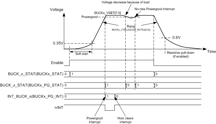
The regulator is enabled by the ENx pin or by I2C writing as shown in Figure 14. The soft-start circuit limits the in-rush current during start-up. When the output voltage rises to 0.35-V level, the output voltage becomes slew-rate controlled using the slew-rate defined by SLEW_RATE[2:0] bits in BUCKx_CTRL2 register. If there is a short circuit at the output and the output voltage does not increase above 0.35-V level in 1 ms, the regulator is disabled, and interrupt is set. When the output voltage reaches the Power-Good threshold level the BUCKx_PG_INT interrupt flag (in INT_BUCK_x register) is set. The Power-Good interrupt flag can be masked using BUCKx_PG_MASK bit (in BUCKx_MASK register).
The ENx input pins have integrated pulldown resistors. The pulldown resistors are enabled by default, and the host can disable those with ENx_PD bits (in CONFIG register).
 Figure 14. Regulator Enable and Disable