ZHCSJ52A December 2019 – August 2021 LP875701-Q1
PRODUCTION DATA
- 1 特性
- 2 应用
- 3 说明
- 4 Revision History
- 5 Pin Configuration and Functions
- 6 Specifications
-
7 Detailed Description
- 7.1 Overview
- 7.2 Functional Block Diagram
- 7.3
Feature Descriptions
- 7.3.1 Multi-Phase DC/DC Converters
- 7.3.2 Sync Clock Functionality
- 7.3.3 Power-Up
- 7.3.4 Regulator Control
- 7.3.5 Enable and Disable Sequences
- 7.3.6 Device Reset Scenarios
- 7.3.7 Diagnosis and Protection Features
- 7.3.8 GPIO Signal Operation
- 7.3.9 Digital Signal Filtering
- 7.4 Device Functional Modes
- 7.5 Programming
- 7.6
Register Maps
- 7.6.1
Register Descriptions
- 53
- 7.6.1.1 DEV_REV
- 7.6.1.2 OTP_REV
- 7.6.1.3 BUCK0_CTRL1
- 7.6.1.4 BUCK0_DELAY
- 7.6.1.5 GPIO2_DELAY
- 7.6.1.6 GPIO3_DELAY
- 7.6.1.7 RESET
- 7.6.1.8 CONFIG
- 7.6.1.9 INT_TOP1
- 7.6.1.10 INT_TOP2
- 7.6.1.11 INT_BUCK_0_1
- 7.6.1.12 INT_BUCK_2_3
- 7.6.1.13 TOP_STAT
- 7.6.1.14 BUCK_0_1_STAT
- 7.6.1.15 BUCK_2_3_STAT
- 7.6.1.16 TOP_MASK1
- 7.6.1.17 TOP_MASK2
- 7.6.1.18 BUCK_0_1_MASK
- 7.6.1.19 BUCK_2_3_MASK
- 7.6.1.20 SEL_I_LOAD
- 7.6.1.21 I_LOAD_2
- 7.6.1.22 I_LOAD_1
- 7.6.1.23 PGOOD_CTRL1
- 7.6.1.24 PGOOD_CTRL2
- 7.6.1.25 PGOOD_FLT
- 7.6.1.26 PLL_CTRL
- 7.6.1.27 PIN_FUNCTION
- 7.6.1.28 GPIO_CONFIG
- 7.6.1.29 GPIO_IN
- 7.6.1.30 GPIO_OUT
- 7.6.1
Register Descriptions
- 8 Application and Implementation
- 9 Power Supply Recommendations
- 10Layout
- 11Device and Documentation Support
- 12Mechanical, Packaging, and Orderable Information
7.3.7.1 Power-Good Information (PGOOD pin)
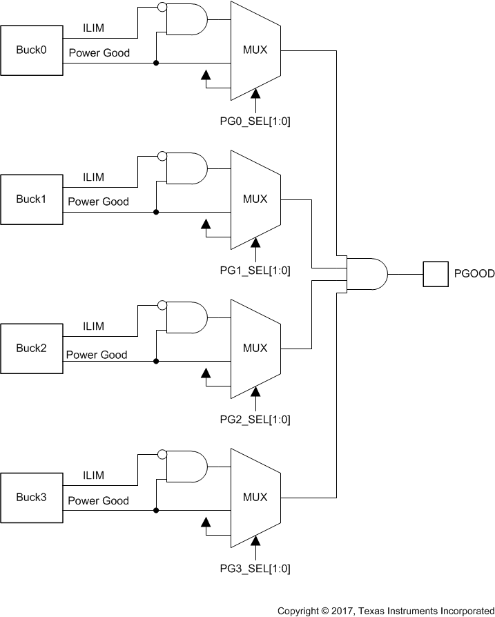
In addition to the interrupt based indication of current limit and Power-Good level the LP875701-Q1 device supports the indication with PGOOD signal. Either voltage and current monitoring or a voltage monitoring only can be selected for PGOOD indication. This selection is individual for all buck regulators (select master phase for multiphase regulator) and is set by PGx_SEL[1:0] bits (in PGOOD_CTRL1 register). When both voltage and current are monitored, PGOOD signal active indicates that regulator output is inside the Power-Good voltage window and that load current is below ILIM FWD. If only voltage is monitored, then the current monitoring is ignored for the PGOOD signal. When a regulator is disabled, the monitoring is automatically masked to prevent it forcing PGOOD inactive. This allows connecting PGOOD signals from various devices together when open-drain outputs are used. When regulator voltage is transitioning from one target voltage to another, the voltage monitoring PGOOD signal is set inactive. The monitoring from all the output rails are combined, and PGOOD is active only if all the sources shows active status. The status from all the voltage rails are summarized in Table 7-6.
If the PGOOD signal is inactive or it changes the state to inactive, the source for the state can be read from PGOOD_FLT register. During reading all the PGx_FLT bit are cleared that are not driving the PGOOD inactive. When PGOOD signal goes active, the host must read the PGOOD_FLT register to clear all the bits. The PGOOD signal follows the status of all the monitored outputs.
The PGOOD signal can be also configured so that it stays in the inactive state even when the monitored outputs are valid but there are PGx_FLT bits pending clearance in PGOOD_FLT register. This mode of operation is selected by setting EN_PGFLT_STAT bit to 1 (in PGOOD_CTRL2 register).
The type of output voltage monitoring for PGOOD signal is selected by PGOOD_WINDOW bit (in PGOOD_CTRL2 register). If the bit is 0, only undervoltage is monitored; if the bit is 1, both undervoltage and overvoltage are monitored.
The polarity and the output type (push-pull or open-drain) are selected by PGOOD_POL and PGOOD_OD bits in PGOOD_CTRL2 register.
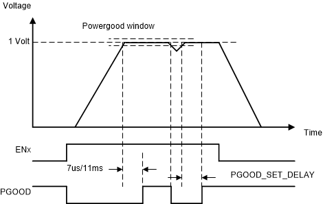
The filtering time for invalid output voltage is always typically 7 µs and for valid output voltage the filtering time is selected with PGOOD_SET_DELAY bit (in PGOOD_CTRL2 register). The Power-Good waveforms are shown in Figure 7-9.
 Figure 7-8 PGOOD Block Diagram
| STATUS / USE CASE | CONDITION | INPUT TO PGOOD SIGNAL |
|---|---|---|
| Buck not selected for PGOOD monitoring | PGx_SEL = 00 (in PGOOD_CTRL1 register) | Active |
| Buck disabled | Active | |
| BUCK SELECTED FOR PGOOD MONITORING | ||
| Buck start-up delay | Inactive | |
| Buck soft start | VOUT < 0.35 V | Inactive |
| Buck voltage ramp-up | 0.35 V < VOUT < VSET | Inactive |
| Output voltage within window limits after start-up | Must be inside limits longer than debounce time | Active |
| Output voltage inside voltage window and current limit active | Current limit active longer than debounce time | Active (if only voltage monitoring selected) Inactive (if also current monitoring selected) |
| Output voltage spikes (overvoltage or undervoltage) | If spikes are outside voltage window longer than debounce time | Inactive |
| Voltage setting change, output voltage ramp | Inactive | |
| Output voltage within window limits after voltage change | Must be inside limits longer than debounce time | Active |
| Buck shutdown delay | Active | |
| Buck output voltage ramp down | Active | |
| Buck disabled by thermal shutdown and interrupt pending | Inactive | |
| Buck disabled by overvoltage and interrupt pending | Inactive | |
| Buck disabled by short-circuit detection and interrupt pending | Inactive | |
 Figure 7-9 PGOOD Waveforms (PGOOD_POL=0)