ZHCSET9B January 2016 – June 2018 LP8758-E0
PRODUCTION DATA.
- 1 特性
- 2 应用
- 3 说明
- 4 修订历史记录
- 5 Pin Configuration and Functions
- 6 Specifications
-
7 Detailed Description
- 7.1 Overview
- 7.2 Functional Block Diagram
- 7.3 Feature Description
- 7.4 Device Functional Modes
- 7.5 Programming
- 7.6
Register Maps
- 7.6.1
Register Descriptions
- 7.6.1.1 OTP_REV
- 7.6.1.2 BUCK0_CTRL1
- 7.6.1.3 BUCK0_CTRL2
- 7.6.1.4 BUCK1_CTRL1
- 7.6.1.5 BUCK1_CTRL2
- 7.6.1.6 BUCK2_CTRL1
- 7.6.1.7 BUCK2_CTRL2
- 7.6.1.8 BUCK3_CTRL1
- 7.6.1.9 BUCK3_CTRL2
- 7.6.1.10 BUCK0_VOUT
- 7.6.1.11 BUCK0_FLOOR_VOUT
- 7.6.1.12 BUCK1_VOUT
- 7.6.1.13 BUCK1_FLOOR_VOUT
- 7.6.1.14 BUCK2_VOUT
- 7.6.1.15 BUCK2_FLOOR_VOUT
- 7.6.1.16 BUCK3_VOUT
- 7.6.1.17 BUCK3_FLOOR_VOUT
- 7.6.1.18 BUCK0_DELAY
- 7.6.1.19 BUCK1_DELAY
- 7.6.1.20 BUCK2_DELAY
- 7.6.1.21 BUCK3_DELAY
- 7.6.1.22 RESET
- 7.6.1.23 CONFIG
- 7.6.1.24 INT_TOP
- 7.6.1.25 INT_BUCK_0_1
- 7.6.1.26 INT_BUCK_2_3
- 7.6.1.27 TOP_STAT
- 7.6.1.28 BUCK_0_1_STAT
- 7.6.1.29 BUCK_2_3_STAT
- 7.6.1.30 TOP_MASK
- 7.6.1.31 BUCK_0_1_MASK
- 7.6.1.32 BUCK_2_3_MASK
- 7.6.1.33 SEL_I_LOAD
- 7.6.1.34 I_LOAD_2
- 7.6.1.35 I_LOAD_1
- 7.6.1
Register Descriptions
- 8 Application and Implementation
- 9 Power Supply Recommendations
- 10Layout
- 11器件和文档支持
- 12机械、封装和可订购信息
7.3.3.1 Enabling and Disabling
The buck converter cores can be enabled when the device is in STANDBY or ACTIVE state. There are two ways for enable and disable the buck converter core cores:
- Using BUCKx_CTRL1.EN_BUCKx register bit (when BUCKx_CTRL1.EN_PIN_CTRLx register bit is 0).
- Using EN1/2 control pins (BUCKx_CTRL1.EN_BUCKx register bit is 1 and BUCKx_CTRL1.EN_PIN_CTRLx register bit is 1).
If the EN1/2 control pins are used for enable and disable, the delay from the control signal rising edge to start-up is set by BUCKx_DELAY.BUCKx_STARTUP_DELAY[3:0] bits and the delay from control signal falling edge to shutdown is set by BUCKx_DELAY.BUCKx_SHUTDOWN_DELAY[3:0] bits. The delays are valid only for EN1/2 signal and not for control with BUCKx_CTRL1.EN_BUCKx bit. The delay time implemented by EN1/2 has overall +/-10% timing accuracy.
The control of the converter cores (with 0 ms delays) is shown in Table 2.
Table 2. Regulator Control
| CONTROL METHOD | ROW | EN_BUCKx | BUCKx_CTRL1
EN_PIN_CTRLx |
BUCKx_CTRL1
EN_PIN_SELECTx |
BUCKx_CTRL1
EN_ROOF_FLOORx |
EN1 PIN | EN2 PIN | BUCKx
OUTPUT VOLTAGE |
|---|---|---|---|---|---|---|---|---|
| Enable/disable control with EN_BUCKx bit | 1 | 0 | Don't Care | Don't Care | Don't Care | Don't Care | Don't Care | Disabled |
| 2 | 1 | 0 | Don't Care | Don't Care | Don't Care | Don't Care | BUCKx_VOUT.BUCKx_VSET[7:0] | |
| Enable/disable control with EN1 pin | 3 | 1 | 1 | 0 | 0 | Low | Don't Care | Disabled |
| 4 | 1 | 1 | 0 | 0 | High | Don't Care | BUCKx_VOUT.BUCKx_VSET[7:0] | |
| Enable/disable control with EN2 pin | 5 | 1 | 1 | 1 | 0 | Don't Care | Low | Disabled |
| 6 | 1 | 1 | 1 | 0 | Don't Care | High | BUCKx_VOUT.BUCKx_VSET[7:0] | |
| Roof/floor control with EN1 pin | 7 | 1 | 1 | 0 | 1 | Low | Don't Care | BUCKx_FLOOR_VOUT.BUCKx_FLOOR_VSET[7:0] |
| 8 | 1 | 1 | 0 | 1 | High | Don't Care | BUCKx_VOUT.BUCKx_VSET[7:0] | |
| Roof/floor control with EN2 pin | 9 | 1 | 1 | 1 | 1 | Don't Care | Low | BUCKx_FLOOR_VOUT.BUCKx_FLOOR_VSET[7:0] |
| 10 | 1 | 1 | 1 | 1 | Don't Care | High | BUCKx_VOUT.BUCKx_VSET[7:0] |
The following configuration allows the enable/disable control using ENx pin:
- BUCKx_CTRL1.EN_BUCKx = 1
- BUCKx_CTRL1.EN_PIN_CTRLx = 1
- BUCKx_CTRL1.EN_ROOF_FLOORx = 0
- BUCKx_VOUT.BUCKx_VSET[7:0] = Required voltage when ENx is high
- The enable pin for control is selected with BUCKx_CTRL1.EN_PIN_SELECTx
When the ENx pin is low, Table 2 row 3 (or 5) is valid, and the converter core is disabled. By setting ENx pin high, Table 2 row 4 (or 6) is valid, and the converter core is enabled with required voltage.
If a converter core is enabled all the time, and the ENx pin controls selection between two voltage level, the following configuration is used:
- BUCKx_CTRL1.EN_BUCKx = 1
- BUCKx_CTRL1.EN_PIN_CTRLx = 1
- BUCKx_CTRL1.EN_ROOF_FLOORx = 1
- BUCKx_VOUT.BUCKx_VSET[7:0] = Required voltage when ENx is high
- The enable pin for control is selected with BUCKx_CTRL1.EN_PIN_SELECTx
When the ENx pin is low, Table 2 row 7 (or 9) is valid, and the core is enabled with a voltage defined by BUCKx_FLOOR_VOUT.BUCKx_FLOOR_VSET[7:0] bits. Setting the ENx pin high, Table 2 row 8 (or 10) is valid, and the core is enabled with a voltage defined by BUCKx_VOUT.BUCKx_VSET[7:0] bits.
If the core is controlled by I2C writings, the BUCKx_CTRL1.EN_PIN_CTRLx bit is set to 0. The enable/disable is controlled by the BUCKx_CTRL1.EN_BUCKx bit, and when the regulator is enabled, the output voltage is defined by the BUCKx_VOUT.BUCKx_VSET[7:0] bits. The Table 2 rows 1 and 2 are valid for I2C controlled operation (ENx pins are ignored).
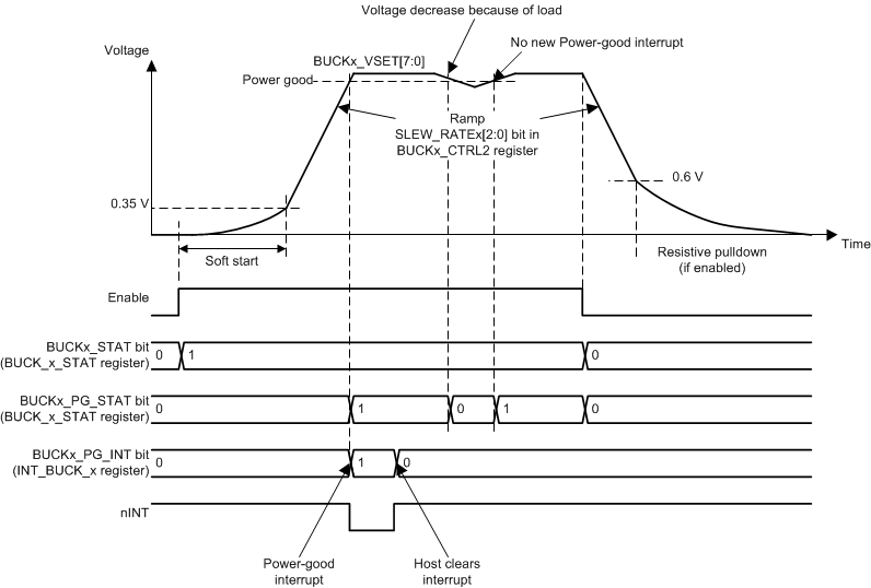
The buck converter core is enabled by the ENx pin or by I2C writing as shown in Figure 9. The soft-start circuit limits the in-rush current during start-up. Output voltage increase rate is around 5 mV/μsec during soft-start. When the output voltage rises to approximately 0.3 V, the output voltage becomes slew-rate controlled. If there is a short circuit at the output, and the output voltage does not increase above a 0.35-V level in 1 ms, the converter core is disabled, and interrupt is set. When the output voltage reaches the powergood threshold level the INT_BUCK_x.BUCKx_PG_INT interrupt flag is set. The powergood interrupt flag can be masked using BUCK_x_MASK.BUCKx_PG_MASK bit.
The ENx input pins have integrated pull-down resistors. The pull-down resistors are enabled by default and host can disable those with CONFIG.ENx_PD bits.
 Figure 9. Converter Core Enable and Disable