SNVSBP2 February   2020 LP8758-E3

PRODUCTION DATA.  

  1. Features
  2. Applications
  3. Description
    1.     Device Images
      1.      Simplified Schematic
      2.      Efficiency vs Output Current
  4. Revision History
  5. Pin Configuration and Functions
    1.     Pin Functions
  6. Specifications
    1. 6.1 Absolute Maximum Ratings
    2. 6.2 ESD Ratings
    3. 6.3 Recommended Operating Conditions
    4. 6.4 Thermal Information
    5. 6.5 Electrical Characteristics
    6. 6.6 I2C Serial Bus Timing Requirements
    7. 6.7 Switching Characteristics
    8. 6.8 Typical Characteristics
  7. Detailed Description
    1. 7.1 Overview
      1. 7.1.1 Buck Information
        1. 7.1.1.1 Operating Modes
        2. 7.1.1.2 Programmability
        3. 7.1.1.3 Features
    2. 7.2 Functional Block Diagram
    3. 7.3 Feature Description
      1. 7.3.1 Overview
        1. 7.3.1.1 Transition between PWM and PFM Modes
        2. 7.3.1.2 Buck Converter Load Current Measurement
        3. 7.3.1.3 Spread-Spectrum Mode
      2. 7.3.2 Power-Up
      3. 7.3.3 Regulator Control
        1. 7.3.3.1 Enabling and Disabling
        2. 7.3.3.2 Changing Output Voltage
      4. 7.3.4 Device Reset Scenarios
      5. 7.3.5 Diagnosis and Protection Features
        1. 7.3.5.1 Warnings for Diagnosis (Interrupt)
          1. 7.3.5.1.1 Output Current Limit
          2. 7.3.5.1.2 Thermal Warning
        2. 7.3.5.2 Protection (Regulator Disable)
          1. 7.3.5.2.1 Short-Circuit and Overload Protection
          2. 7.3.5.2.2 Thermal Shutdown
        3. 7.3.5.3 Fault (Power Down)
          1. 7.3.5.3.1 Undervoltage Lockout
      6. 7.3.6 Digital Signal Filtering
    4. 7.4 Device Functional Modes
      1. 7.4.1 Modes of Operation
    5. 7.5 Programming
      1. 7.5.1 I2C-Compatible Interface
        1. 7.5.1.1 Data Validity
        2. 7.5.1.2 Start and Stop Conditions
        3. 7.5.1.3 Transferring Data
        4. 7.5.1.4 I2C-Compatible Chip Address
        5. 7.5.1.5 Auto Increment Feature
    6. 7.6 Register Maps
      1. 7.6.1 Register Descriptions
        1. 7.6.1.1  OTP_REV
        2. 7.6.1.2  BUCK0_CTRL1
        3. 7.6.1.3  BUCK0_CTRL2
        4. 7.6.1.4  BUCK1_CTRL1
        5. 7.6.1.5  BUCK1_CTRL2
        6. 7.6.1.6  BUCK2_CTRL1
        7. 7.6.1.7  BUCK2_CTRL2
        8. 7.6.1.8  BUCK3_CTRL1
        9. 7.6.1.9  BUCK3_CTRL2
        10. 7.6.1.10 BUCK0_VOUT
        11. 7.6.1.11 BUCK0_FLOOR_VOUT
        12. 7.6.1.12 BUCK1_VOUT
        13. 7.6.1.13 BUCK1_FLOOR_VOUT
        14. 7.6.1.14 BUCK2_VOUT
        15. 7.6.1.15 BUCK2_FLOOR_VOUT
        16. 7.6.1.16 BUCK3_VOUT
        17. 7.6.1.17 BUCK3_FLOOR_VOUT
        18. 7.6.1.18 BUCK0_DELAY
        19. 7.6.1.19 BUCK1_DELAY
        20. 7.6.1.20 BUCK2_DELAY
        21. 7.6.1.21 BUCK3_DELAY
        22. 7.6.1.22 RESET
        23. 7.6.1.23 CONFIG
        24. 7.6.1.24 INT_TOP
        25. 7.6.1.25 INT_BUCK_0_1
        26. 7.6.1.26 INT_BUCK_2_3
        27. 7.6.1.27 TOP_STAT
        28. 7.6.1.28 BUCK_0_1_STAT
        29. 7.6.1.29 BUCK_2_3_STAT
        30. 7.6.1.30 TOP_MASK
        31. 7.6.1.31 BUCK_0_1_MASK
        32. 7.6.1.32 BUCK_2_3_MASK
        33. 7.6.1.33 SEL_I_LOAD
        34. 7.6.1.34 I_LOAD_2
        35. 7.6.1.35 I_LOAD_1
  8. Application and Implementation
    1. 8.1 Application Information
    2. 8.2 Typical Application
      1. 8.2.1 Design Requirements
      2. 8.2.2 Detailed Design Procedure
        1. 8.2.2.1 Application Components
          1. 8.2.2.1.1 Inductor Selection
          2. 8.2.2.1.2 Input Capacitor Selection
          3. 8.2.2.1.3 Output Capacitor Selection
      3. 8.2.3 Application Curves
  9. Power Supply Recommendations
  10. 10Layout
    1. 10.1 Layout Guidelines
    2. 10.2 Layout Example
  11. 11Device and Documentation Support
    1. 11.1 Device Support
      1. 11.1.1 Third-Party Products Disclaimer
    2. 11.2 Documentation Support
      1. 11.2.1 Related Documentation
    3. 11.3 Receiving Notification of Documentation Updates
    4. 11.4 Community Resources
    5. 11.5 Trademarks
    6. 11.6 Electrostatic Discharge Caution
    7. 11.7 Glossary
  12. 12Mechanical, Packaging, and Orderable Information

封装选项

机械数据 (封装 | 引脚)
散热焊盘机械数据 (封装 | 引脚)
订购信息

Application Curves

Measurements are done using typical application set up with connections shown in Figure 19. Graphs may not reflect the OTP default settings. Unless otherwise specified: VIN = 3.7 V, V(NRST) = 1.8 V, TA = 25 °C, ƒSW = 3 MHz, L = 470 nH (TDK VLS252010HBX-R47M), ILIM FWD set to maximum 5 A.
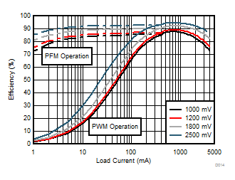
LP8758-E3 D014_EFFI_SNVSAC6.gif
VIN = 3.7 V
VOUT settings = 1000 mV, 1200 mV, 1800 mV, and 2500 mV
Figure 20. Efficiency vs Load Current
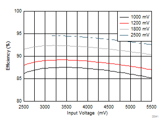
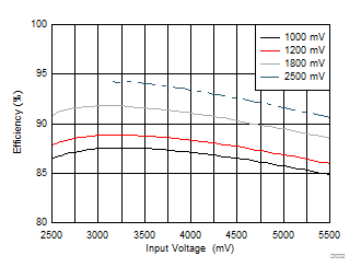
LP8758-E3 D041_EFFI_VIN_PWM_SNVSAC6.gif
Load = 1A
VOUT settings = 1000 mV, 1200 mV, 1800 mV, and 2500 mV
Figure 22. Efficiency vs Input Voltage in PWM Mode
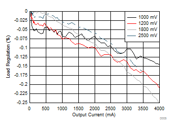
LP8758-E3 D005_PWM_LOADREG_SNVSAC6.gif
Change in Output Voltage from Zero Load (%)
VOUT settings = 1000 mV, 1200 mV, 1800 mV, and 2500 mV
Figure 24. DC Load Regulation in PWM mode
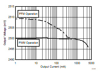
LP8758-E3 D046_VO2v5_VS_LOAD_SNVSAC6.gif
VOUT setting = 2500 mV
Figure 26. Output Voltage vs Load Current in
PWM-PFM Mode
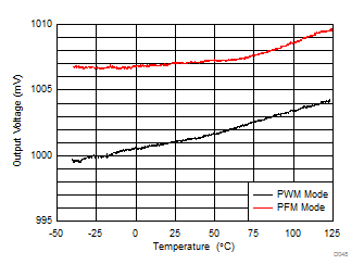
LP8758-E3 D048_VOUT_vs_TEMP_SNVSAC6.gif
VOUT setting = 1000 mV
Load = 1 A (PWM Mode) and 100 mA (PFM Mode)
Figure 28. Output Voltage vs Temperature
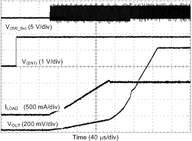
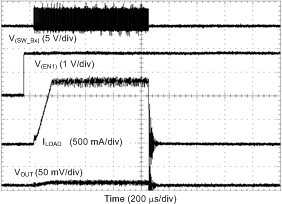
LP8758-E3 start_1A_LOAD_SNVSAC6.gif
Load = 1 A
Figure 30. Start-up with EN1
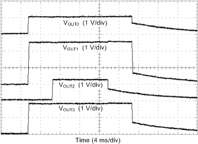
LP8758-E3 default_start_SNVSAC6.gif
Load = 0 A Enable and disable delays = default
VOUT settings = default
Figure 32. VOUT0,1,2,3: Start-up and Shutdown with Default Register Settings, triggered by EN1.
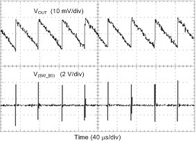
LP8758-E3 PFM_ripple_voltage.gif
Load = 10 mA
Figure 34. Output Voltage Ripple, PFM Mode
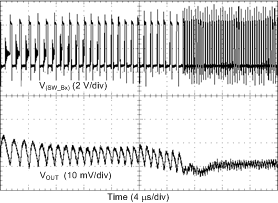
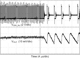
LP8758-E3 PFM_to_PWM_SNVSAC6.gif
Figure 36. Transient from PFM-to-PWM Mode
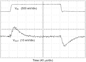
LP8758-E3 line_tran_3v3_3v8.gif
Load = 4 A VOUT = 1000 mV
VIN stepping 3.3 V ↔ 3.8 V, TR = TF = 10 µs
Figure 38. Transient Line Response
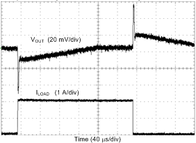
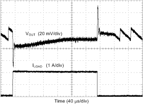
LP8758-E3 PWM_LOAD_TRAN_0A_2A_400ns.gif
Load = 0 A → 2 A → 0 A TR = TF = 400 ns VOUT = 1 V
Figure 40. Transient Load Step Response,
Forced PWM Mode
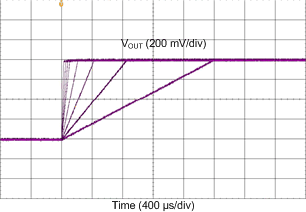
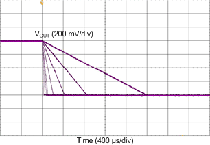
LP8758-E3 D026_slewrate.gif
Figure 42. VOUT Transition From 0.6 V to 1.4 V With Different Slew Rate Settings
LP8758-E3 D002_EFFI_VIN_PFM_SNVSAC6.gif
Load = 100 mA
VOUT settings = 1000 mV, 1200 mV, 1800 mV, and 2500 mV
Figure 21. Efficiency vs Input Voltage in PFM Mode
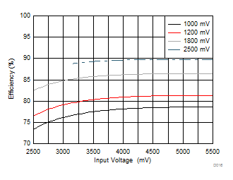
LP8758-E3 D016_EFFI_VIN_PWM_SNVSAC6.gif
Load = 3A
VOUT settings = 1000 mV, 1200 mV, 1800 mV, and 2500 mV
Figure 23. Efficiency vs Input Voltage in PWM Mode
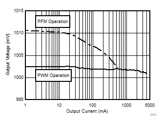
LP8758-E3 D047_VO1v0_VS_LOAD_SNVSAC6.gif
VOUT setting = 1000 mV
Figure 25. Output Voltage vs Load Current in
PWM-PFM Mode
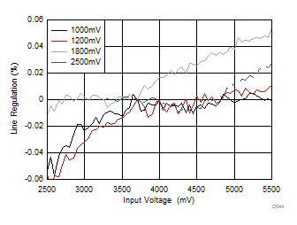
LP8758-E3 LINEREG_SNVSAC6.gif
Change in Output Voltage from VIN = 3.7 V (%) Load = 1 A
VOUT settings = 1000 mV, 1200 mV, 1800 mV, and 2500 mV
Figure 27. DC Line Regulation in PWM Mode
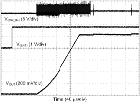
LP8758-E3 start_0A_LOAD_SNVSAC6.gif
Load = 0 A
Figure 29. Start-up with EN1
LP8758-E3 start_with_short_SNVSAC6.gif
Figure 31. Start-up With Short on Output
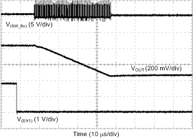
LP8758-E3 Shutdown_SNVSAC6.gif
Load = 0 A
Figure 33. Shutdown with EN1
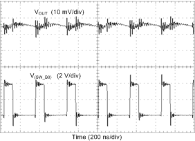
LP8758-E3 PWM_ripple_voltage.gif
Load = 200 mA
Figure 35. Output Voltage Ripple, Forced PWM Mode
LP8758-E3 PWM_to_PFM_SNVSAC6.gif
Figure 37. Transient from PWM-to-PFM Mode
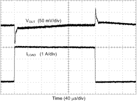
LP8758-E3 PFM_LOAD_TRAN_0A_2A_400ns.gif
Load = 0 A → 2 A → 0 A TR = TF = 400 ns VOUT = 1 V
Figure 39. Transient Load Step Response, AUTO Mode
LP8758-E3 PWM_LOAD_TRAN_1A_4A_1us.gif
Load = 1A → 4 A → 1A TR = TF = 1 µs VOUT = 1 V
Figure 41. Transient Load Step Response,
Forced PWM Mode
LP8758-E3 D042_slewrate_down.gif
Figure 43. VOUT Transition From 1.4 V to 0.6 V With Different Slew Rate Settings