SNVSBP2 February   2020 LP8758-E3

PRODUCTION DATA.  

  1. Features
  2. Applications
  3. Description
    1.     Device Images
      1.      Simplified Schematic
      2.      Efficiency vs Output Current
  4. Revision History
  5. Pin Configuration and Functions
    1.     Pin Functions
  6. Specifications
    1. 6.1 Absolute Maximum Ratings
    2. 6.2 ESD Ratings
    3. 6.3 Recommended Operating Conditions
    4. 6.4 Thermal Information
    5. 6.5 Electrical Characteristics
    6. 6.6 I2C Serial Bus Timing Requirements
    7. 6.7 Switching Characteristics
    8. 6.8 Typical Characteristics
  7. Detailed Description
    1. 7.1 Overview
      1. 7.1.1 Buck Information
        1. 7.1.1.1 Operating Modes
        2. 7.1.1.2 Programmability
        3. 7.1.1.3 Features
    2. 7.2 Functional Block Diagram
    3. 7.3 Feature Description
      1. 7.3.1 Overview
        1. 7.3.1.1 Transition between PWM and PFM Modes
        2. 7.3.1.2 Buck Converter Load Current Measurement
        3. 7.3.1.3 Spread-Spectrum Mode
      2. 7.3.2 Power-Up
      3. 7.3.3 Regulator Control
        1. 7.3.3.1 Enabling and Disabling
        2. 7.3.3.2 Changing Output Voltage
      4. 7.3.4 Device Reset Scenarios
      5. 7.3.5 Diagnosis and Protection Features
        1. 7.3.5.1 Warnings for Diagnosis (Interrupt)
          1. 7.3.5.1.1 Output Current Limit
          2. 7.3.5.1.2 Thermal Warning
        2. 7.3.5.2 Protection (Regulator Disable)
          1. 7.3.5.2.1 Short-Circuit and Overload Protection
          2. 7.3.5.2.2 Thermal Shutdown
        3. 7.3.5.3 Fault (Power Down)
          1. 7.3.5.3.1 Undervoltage Lockout
      6. 7.3.6 Digital Signal Filtering
    4. 7.4 Device Functional Modes
      1. 7.4.1 Modes of Operation
    5. 7.5 Programming
      1. 7.5.1 I2C-Compatible Interface
        1. 7.5.1.1 Data Validity
        2. 7.5.1.2 Start and Stop Conditions
        3. 7.5.1.3 Transferring Data
        4. 7.5.1.4 I2C-Compatible Chip Address
        5. 7.5.1.5 Auto Increment Feature
    6. 7.6 Register Maps
      1. 7.6.1 Register Descriptions
        1. 7.6.1.1  OTP_REV
        2. 7.6.1.2  BUCK0_CTRL1
        3. 7.6.1.3  BUCK0_CTRL2
        4. 7.6.1.4  BUCK1_CTRL1
        5. 7.6.1.5  BUCK1_CTRL2
        6. 7.6.1.6  BUCK2_CTRL1
        7. 7.6.1.7  BUCK2_CTRL2
        8. 7.6.1.8  BUCK3_CTRL1
        9. 7.6.1.9  BUCK3_CTRL2
        10. 7.6.1.10 BUCK0_VOUT
        11. 7.6.1.11 BUCK0_FLOOR_VOUT
        12. 7.6.1.12 BUCK1_VOUT
        13. 7.6.1.13 BUCK1_FLOOR_VOUT
        14. 7.6.1.14 BUCK2_VOUT
        15. 7.6.1.15 BUCK2_FLOOR_VOUT
        16. 7.6.1.16 BUCK3_VOUT
        17. 7.6.1.17 BUCK3_FLOOR_VOUT
        18. 7.6.1.18 BUCK0_DELAY
        19. 7.6.1.19 BUCK1_DELAY
        20. 7.6.1.20 BUCK2_DELAY
        21. 7.6.1.21 BUCK3_DELAY
        22. 7.6.1.22 RESET
        23. 7.6.1.23 CONFIG
        24. 7.6.1.24 INT_TOP
        25. 7.6.1.25 INT_BUCK_0_1
        26. 7.6.1.26 INT_BUCK_2_3
        27. 7.6.1.27 TOP_STAT
        28. 7.6.1.28 BUCK_0_1_STAT
        29. 7.6.1.29 BUCK_2_3_STAT
        30. 7.6.1.30 TOP_MASK
        31. 7.6.1.31 BUCK_0_1_MASK
        32. 7.6.1.32 BUCK_2_3_MASK
        33. 7.6.1.33 SEL_I_LOAD
        34. 7.6.1.34 I_LOAD_2
        35. 7.6.1.35 I_LOAD_1
  8. Application and Implementation
    1. 8.1 Application Information
    2. 8.2 Typical Application
      1. 8.2.1 Design Requirements
      2. 8.2.2 Detailed Design Procedure
        1. 8.2.2.1 Application Components
          1. 8.2.2.1.1 Inductor Selection
          2. 8.2.2.1.2 Input Capacitor Selection
          3. 8.2.2.1.3 Output Capacitor Selection
      3. 8.2.3 Application Curves
  9. Power Supply Recommendations
  10. 10Layout
    1. 10.1 Layout Guidelines
    2. 10.2 Layout Example
  11. 11Device and Documentation Support
    1. 11.1 Device Support
      1. 11.1.1 Third-Party Products Disclaimer
    2. 11.2 Documentation Support
      1. 11.2.1 Related Documentation
    3. 11.3 Receiving Notification of Documentation Updates
    4. 11.4 Community Resources
    5. 11.5 Trademarks
    6. 11.6 Electrostatic Discharge Caution
    7. 11.7 Glossary
  12. 12Mechanical, Packaging, and Orderable Information

封装选项

机械数据 (封装 | 引脚)
散热焊盘机械数据 (封装 | 引脚)
订购信息

Spread-Spectrum Mode

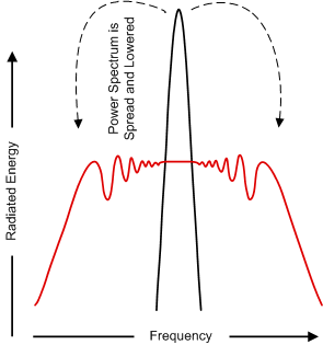
Systems with periodic switching signals may generate a large amount of switching noise in a set of narrowband frequencies (the switching frequency and its harmonics). The usual solution to reduce noise coupling is to add EMI-filters and shields to the boards. The register-selectable spread-spectrum mode of the device minimizes the need for output filters, ferrite beads, or chokes. In spread-spectrum mode, the switching frequency varies randomly by ±5% about the center frequency, reducing the EMI emissions radiated by the converter and associated passive components and PCB traces (see Figure 8). This feature is enabled with the CONFIG.EN_SPREAD_SPEC bit, and it affects all the buck converter cores.
LP8758-E3 30190611.gif
Where a fixed frequency converter exhibits large amounts of spectral energy at the switching frequency, the spread spectrum architecture of the v spreads that energy over a large bandwidth.
Figure 8. Spread-Spectrum Modulation