ZHCSIH0C December 2017 – June 2021 LP87702-Q1
PRODUCTION DATA
- 1 特性
- 2 应用
- 3 说明
- 4 Revision History
- 5 说明(续)
- 6 Pin Configuration and Functions
- 7 Specifications
-
8 Detailed Description
- 8.1 Overview
- 8.2 Functional Block Diagram
- 8.3
Feature Descriptions
- 8.3.1 Step-Down DC/DC Converters
- 8.3.2 Boost Converter
- 8.3.3 Spread-Spectrum Mode
- 8.3.4 Sync Clock Functionality
- 8.3.5 Power-Up
- 8.3.6 Buck and Boost Control
- 8.3.7 Enable and Disable Sequences
- 8.3.8 Window Watchdog
- 8.3.9 Device Reset Scenarios
- 8.3.10 Diagnostics and Protection Features
- 8.3.11 OTP Error Correction
- 8.3.12 Operation of GPO Signals
- 8.3.13 Digital Signal Filtering
- 8.4 Device Functional Modes
- 8.5 Programming
- 8.6 Register Maps
- 9 Application and Implementation
- 10Power Supply Recommendations
- 11Layout
- 12Device and Documentation Support
- 13Mechanical, Packaging, and Orderable Information
8.3.10.3.2 PGx Pin Operation in Continuous Mode
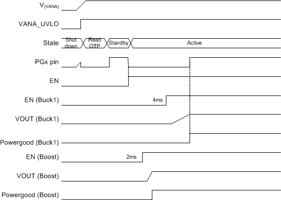
In this mode the PGx signal shows the validity of the requested voltages continuously. Mode is selected by setting the PGx_MODE bit to 1 in the PG_CTRL register.
For the continuous mode of operation, the PGx behaves as follows:
- PGx is set to active or asserted state upon exiting the OTP configuration as an initial default state.
- PGx is set to inactive or de-asserted as soon as the converter is enabled.
- PGx status begins indicating the output voltage regulation status immediately and continuously.
- PGx state changes between inactive or deasserted and active or asserted during power-up sequencing and requested voltage changes, depending on the output voltages being outside or inside of the regualtion ranges.
When an invalid output voltage of monitored converter is detected, the corresponding bit in the PG0_FAULT or PG1_FAULT register is set to 1 and the PGx signal becomes inactive. The PG0_FAULT and PG1_FAULT register bits are latched and maintain the fault information until host clears the fault bit by writing 1 to the bit. The PGx signal also indicates the interrupts from VANA, VMON1, and VMON2 inputs and thermal warning and shutdown. All are cleared by clearing the interrupt bits.
The PGx signal is set inactive when the converter voltage is transitioning from one target voltage to another.
The source for the fault can be read from PGx_FAULT register when PGx signal becomes inactive. If the invalid output voltage becomes valid again the PGx signal becomes active. Thus the PGx signal shows all the time if the monitored output voltages are valid. Figure 8-11 shows an example of the PGx pin operation in continuous mode.
The PGx signal can also be configured so that it maintains the inactive state even when the monitored outputs are valid, but there are PG_FAULT_x bits pending clearance. This type of operation is selected by setting the PGOOD_FAULT_GATES_PGx bit to 1.
 Figure 8-11 PGx Pin
Operation in Continuous Mode