ZHCSIH0C December   2017  – June 2021 LP87702-Q1

PRODUCTION DATA  

  1. 特性
  2. 应用
  3. 说明
  4. Revision History
  5. 说明(续)
  6. Pin Configuration and Functions
  7. Specifications
    1. 7.1 Absolute Maximum Ratings
    2. 7.2 ESD Ratings
    3. 7.3 Recommended Operating Conditions
    4. 7.4 Thermal Information
    5. 7.5 Electrical Characteristics
    6. 7.6 I2C Serial Bus Timing Parameters
    7. 7.7 Typical Characteristics
  8. Detailed Description
    1. 8.1 Overview
    2. 8.2 Functional Block Diagram
    3. 8.3 Feature Descriptions
      1. 8.3.1  Step-Down DC/DC Converters
        1. 8.3.1.1 Overview
        2. 8.3.1.2 Transition Between PWM and PFM Modes
        3. 8.3.1.3 Buck Converter Load Current Measurement
      2. 8.3.2  Boost Converter
      3. 8.3.3  Spread-Spectrum Mode
      4. 8.3.4  Sync Clock Functionality
      5. 8.3.5  Power-Up
      6. 8.3.6  Buck and Boost Control
        1. 8.3.6.1 Enabling and Disabling Converters
        2. 8.3.6.2 Changing Buck Output Voltage
      7. 8.3.7  Enable and Disable Sequences
      8. 8.3.8  Window Watchdog
      9. 8.3.9  Device Reset Scenarios
      10. 8.3.10 Diagnostics and Protection Features
        1. 8.3.10.1 Voltage Monitorings
        2. 8.3.10.2 Interrupts
        3. 8.3.10.3 Power-Good Information to Interrupt, PG0, and PG1 Pins
          1. 8.3.10.3.1 PGx Pin Gated (Unusual) Mode
          2. 8.3.10.3.2 PGx Pin Operation in Continuous Mode
          3. 8.3.10.3.3 Summary of PG0, PG1 Gated, and Continuous Operating Modes
        4. 8.3.10.4 Warning Interrupts for System Level Diagnostics
          1. 8.3.10.4.1 Output Power Limit
          2. 8.3.10.4.2 Thermal Warning
        5. 8.3.10.5 Protections Causing Converter Disable
          1. 8.3.10.5.1 Short-Circuit and Overload Protection
          2. 8.3.10.5.2 Overvoltage Protection
          3. 8.3.10.5.3 Thermal Shutdown
        6. 8.3.10.6 Protections Causing Device Power Down
          1. 8.3.10.6.1 Undervoltage Lockout
      11. 8.3.11 OTP Error Correction
      12. 8.3.12 Operation of GPO Signals
      13. 8.3.13 Digital Signal Filtering
    4. 8.4 Device Functional Modes
      1. 8.4.1 Modes of Operation
    5. 8.5 Programming
      1. 8.5.1 I2C-Compatible Interface
        1. 8.5.1.1 Data Validity
        2. 8.5.1.2 Start and Stop Conditions
        3. 8.5.1.3 Transferring Data
        4. 8.5.1.4 I2C-Compatible Chip Address
        5. 8.5.1.5 Auto Increment Feature
    6. 8.6 Register Maps
      1. 8.6.1 Register Descriptions
        1. 8.6.1.1 LP8770_map Registers
  9. Application and Implementation
    1. 9.1 Application Information
    2. 9.2 Typical Application
      1. 9.2.1 Design Requirements
      2. 9.2.2 Detailed Design Procedure
        1. 9.2.2.1 Application Components
          1. 9.2.2.1.1 Inductor Selection
          2. 9.2.2.1.2 Buck Input Capacitor Selection
          3. 9.2.2.1.3 Buck Output Capacitor Selection
          4. 9.2.2.1.4 Boost Input Capacitor Selection
          5. 9.2.2.1.5 Boost Output Capacitor Selection
          6. 9.2.2.1.6 Supply Filtering Components
      3. 9.2.3 Current Limit vs Maximum Output Current
      4. 9.2.4 Application Curves
  10. 10Power Supply Recommendations
  11. 11Layout
    1. 11.1 Layout Guidelines
    2. 11.2 Layout Example
  12. 12Device and Documentation Support
    1. 12.1 第三方米6体育平台手机版_好二三四免责声明
    2. 12.2 Receiving Notification of Documentation Updates
    3. 12.3 支持资源
    4. 12.4 Trademarks
    5. 12.5 Electrostatic Discharge Caution
    6. 12.6 Glossary
  13. 13Mechanical, Packaging, and Orderable Information

封装选项

机械数据 (封装 | 引脚)
散热焊盘机械数据 (封装 | 引脚)
订购信息

Data Validity

The data on the SDA line must be stable during the HIGH period of the clock signal (SCL). In other words, the state of the data line can only be changed when clock signal is LOW.
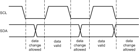
GUID-D29315B5-2C90-44E3-AAC2-2E676747E462-low.gifFigure 8-15 Data Validity Diagram