ZHCSIH0C December 2017 – June 2021 LP87702-Q1
PRODUCTION DATA
- 1 特性
- 2 应用
- 3 说明
- 4 Revision History
- 5 说明(续)
- 6 Pin Configuration and Functions
- 7 Specifications
-
8 Detailed Description
- 8.1 Overview
- 8.2 Functional Block Diagram
- 8.3
Feature Descriptions
- 8.3.1 Step-Down DC/DC Converters
- 8.3.2 Boost Converter
- 8.3.3 Spread-Spectrum Mode
- 8.3.4 Sync Clock Functionality
- 8.3.5 Power-Up
- 8.3.6 Buck and Boost Control
- 8.3.7 Enable and Disable Sequences
- 8.3.8 Window Watchdog
- 8.3.9 Device Reset Scenarios
- 8.3.10 Diagnostics and Protection Features
- 8.3.11 OTP Error Correction
- 8.3.12 Operation of GPO Signals
- 8.3.13 Digital Signal Filtering
- 8.4 Device Functional Modes
- 8.5 Programming
- 8.6 Register Maps
- 9 Application and Implementation
- 10Power Supply Recommendations
- 11Layout
- 12Device and Documentation Support
- 13Mechanical, Packaging, and Orderable Information
8.3.10.3.1 PGx Pin Gated (Unusual) Mode
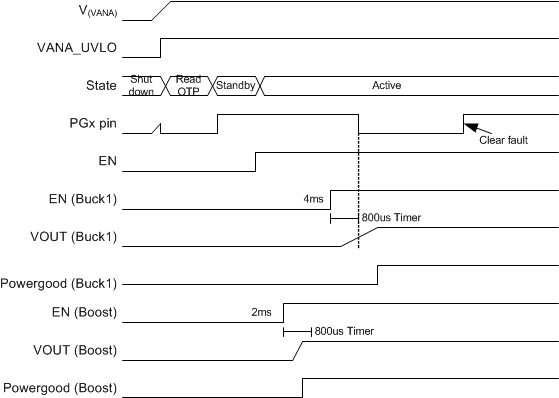
The PGx signal detects unexpected or unusual situations in this mode. Mode is selected by setting the PGx_MODE bit to 0 in the PG_CTRL register.
For the gated mode of operation, the PGx behaves as follows:
- PGx is set to active or asserted state upon exiting the OTP configuration as an initial default state.
- The PGx status is active or asserted during an 800-μs gated time period from the enable activation for each enabled rail, thereby gating-off the status indication.
- The PGx state typically remains active or asserted for normal conditions during normal power-up sequencing and requested voltage changes.
- The PGx status could change to inactive or de-asserted after an 800-μs gated time period if any output voltage is outside of regulation range during an abnormal power-up sequencing and requested voltage changes.
- Using the gated mode of operation could allow the PGx signal to initiate an immediate power shutdown sequence if the PGx signal is wired-OR with signal connected to the EN input. This type of circuit configuration provides a smart PORz function for processor that eliminates the need for additional components to generate PORz upon start-up and to monitor voltage levels of key voltage domains.
PGx signal is set inactive if the output voltage of a monitored buck or boost converter is invalid or the output voltage is not valid at 800 µs from the enable of the converter, which should be considered when selecting the BUCKx_SLEW_RATE setting. Keep the sum of the soft start time and slew rate controlled part of the voltage ramp below 800 µs to avoid PGx triggering at start-up. In addition, the PGx is inactive when the invalid input voltage at VANA, VMON1, or VMON2 pin is detected.
Detected fault sets the corresponding fault bit in PG0_FAULT or in PG1_FAULT register. The detected fault must be cleared to continue the PGx monitoring. The over-voltage and thermal faults are cleared by writing 1 to the corresponding interrupt bits in INT_TOP_1 register. Converter, VMONx and VANA faults are cleared by writing 1 to the corresponding register bit in INT_BUCK, INT_BOOST, and INT_DIAG register, respectively. An example of the PGx pin operation in gated mode is shown in Figure 8-10 and the different use cases for the PGx signal operation are summarized in Table 8-6.
 Figure 8-10 PGx Pin Operation in Gated Mode.